Actinic inspection
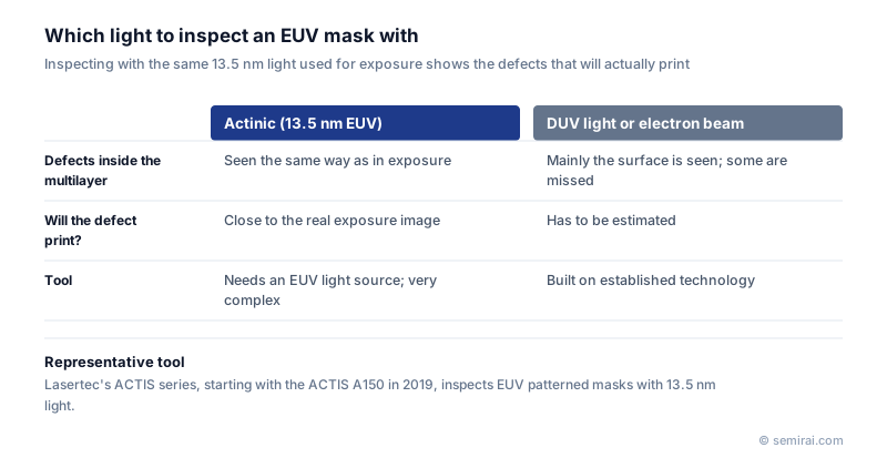
Actinic inspection means inspecting an EUV photomask with the same 13.5 nm extreme ultraviolet light used to expose wafers. Because the inspection light behaves like the exposure light, it finds the mask defects that will actually print on the wafer.
Also called: Actinic EUV mask inspection, APMI
Diagram
Why EUV masks need it
EUV masks do not let light pass through. They reflect it with a mirror made of many thin alternating layers, with the circuit pattern formed in an absorber on top. A defect buried inside that multilayer mirror can disturb the reflected light and print on the wafer, even if the surface looks clean.
Inspection tools that use deep ultraviolet (DUV) light or electron beams mainly see the surface and cannot detect such phase defects reliably. Inspecting with 13.5 nm light shows the mask as the scanner will see it.
The tools
Lasertec released the ACTIS A150 in 2019, which it describes as the world's first actinic EUV patterned mask inspection system. In October 2025 it announced the ACTIS A200HiT series, with three times the inspection speed of the A150, for checking EUV masks when they arrive at a wafer fab and periodically during use.
Building such a tool requires its own EUV light source and reflective optics, which is why actinic inspection arrived years after EUV lithography itself.
Japanese companies involved
- Lasertec, a Japanese company, makes the ACTIS series and is the company most associated with actinic patterned mask inspection.
- The masks themselves start from mask blanks, where Japan's HOYA and AGC are the main suppliers for EUV.
Related pages
Sources
Last updated: October 22, 2026