CMOS under Array (CUA) and CMOS Bonded Array (CBA)
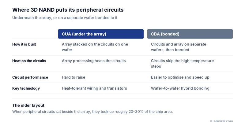
CMOS under Array (CUA) and CMOS Bonded Array (CBA) are 3D NAND architectures that place the peripheral circuits, such as page buffers, sense amplifiers and decoders, directly beneath the memory cell array rather than beside it. This frees the chip area that peripheral circuits used to occupy, raising the share of the die that stores data.
Also called: CuA, CBA, CMOS directly Bonded to Array, Xtack
Diagram
CMOS under Array
In CUA, the CMOS peripheral circuits are built first on the wafer and the memory array is then stacked on top of them on the same wafer. Micron has used this approach since the 3D NAND generations it developed with Intel.
The drawback is heat. Building the cell stack involves high-temperature steps, and the CMOS transistors underneath have to survive them, which limits how fast those circuits can be made.
CMOS Bonded Array
In CBA, the peripheral circuits and the memory array are made on two separate wafers, each with its own optimised process. The wafers are then bonded face to face with copper-to-copper hybrid bonding, connecting millions of contacts at once.
Because the CMOS wafer never sees the array's high-temperature steps, its transistors can be faster, which helps raise interface speed. Kioxia and Western Digital introduced CBA in their eighth-generation BiCS FLASH, and YMTC's Xtack uses the same principle. Wafer-to-wafer bonding of this kind is also being considered for future 3D DRAM.
Both approaches change how 3D NAND chips are laid out. With the peripheral circuits out of the way, the area taken by each memory plane shrinks, and the chip can be divided into more planes that operate in parallel, which improves throughput.
Japanese companies involved
- Kioxia, with Western Digital, adopted CMOS directly Bonded to Array (CBA) in its eighth-generation BiCS FLASH 3D NAND.
- Kioxia · NAND flash memory and SSDs
FAQ
What is the main difference between CUA and CBA?
CUA builds the memory array on top of the circuits on the same wafer; CBA builds them on separate wafers and bonds them together, so each can be optimised separately.
How are the wafers joined in CBA?
By wafer-to-wafer hybrid bonding, in which copper pads and the surrounding dielectric on the two wafers are bonded directly without solder bumps.
Related pages
Sources
Last updated: November 2, 2026