Wafer Bonding
Wafer bonding is the joining of two wafers, or of dies to a wafer, into one permanent or temporary structure, usually with the patterns on both sides aligned to each other. Depending on the method, the surfaces bond directly, through a metal layer or through an adhesive. It is used to make SOI wafers, MEMS, backside-illuminated and stacked image sensors and 3D ICs.
Also called: direct bonding, fusion bonding, hybrid bonding, anodic bonding
Diagram
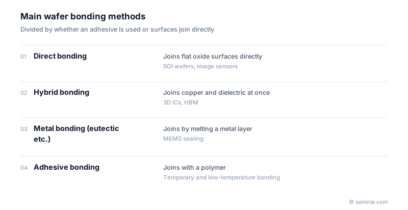
Main bonding methods
Direct or fusion bonding joins two very flat, clean surfaces, typically silicon oxide to oxide or silicon, with no intermediate layer. After plasma activation, the wafers stick on contact through weak surface forces, and an anneal converts these into strong covalent bonds. This is how SOI wafers and many stacked image sensors are made.
Anodic bonding joins silicon to a glass containing sodium, at a few hundred degrees with a high voltage applied, and is widely used to seal MEMS sensors. Metal bonding uses eutectic alloys such as gold-tin or aluminium-germanium, or thermocompression of copper or gold, and gives hermetic seals and electrical contact. Adhesive bonding uses polymers such as BCB or epoxy; it tolerates rougher surfaces and works at low temperature, and is the basis of temporary bonding to carrier wafers during thinning.
Hybrid bonding
Hybrid bonding joins a dielectric surface and the copper pads embedded in it in one step. The two surfaces are polished by CMP so that the copper pads sit very slightly below the oxide. The oxide bonds first at room temperature, and an anneal makes the copper expand and fuse across the gap. Because no solder is involved, pad pitches can drop below 10 µm, far finer than micro-bumps.
Sony brought copper-to-copper hybrid bonding into volume production for stacked CMOS image sensors, and it is now used for logic-on-logic and cache-on-processor stacking such as TSMC SoIC and AMD's 3D V-Cache. It is also studied for future HBM generations. Die-to-wafer hybrid bonding, where individual known-good dies are placed on a wafer, is harder than wafer-to-wafer bonding because each die must be kept free of particles after dicing.
What decides bond quality
Surface flatness, cleanliness and alignment matter most. A single particle can leave a void millimetres across, and roughness above a fraction of a nanometre prevents direct bonding. Fine-pitch bonds need overlay between the two wafers well below a micrometre, and differences in thermal expansion or wafer bow cause distortion. Voids are checked with infrared or acoustic microscopy.
Japanese companies involved
- Tokyo Electron makes wafer bonding and debonding systems for permanent and temporary bonding.
- Sony Semiconductor Solutions was the first to mass-produce image sensors that use copper-to-copper hybrid bonding between the pixel and logic wafers.
- Tokyo Electron (TEL) · Coat/develop, etch and deposition equipment
- Sony Semiconductor Solutions · CMOS image sensors
FAQ
What is the difference between wafer-to-wafer and die-to-wafer bonding?
Wafer-to-wafer bonding joins two whole wafers at once, which is fast and precise but requires both wafers to have the same die size and accepts that a bad die may be bonded to a good one. Die-to-wafer bonding places tested dies one by one, allowing different die sizes and better yield at the cost of throughput.
Is temporary bonding a kind of wafer bonding?
Yes. A device wafer is attached to a glass or silicon carrier with an adhesive so it can be thinned and processed on the back, then released by laser, heat or mechanical debonding. The adhesive must survive processing yet come away cleanly.
What is surface activated bonding?
A room-temperature method in which surfaces are cleaned in vacuum by an ion or atom beam, exposing dangling bonds that join directly on contact. It can bond dissimilar materials that would crack if annealed together.
Related pages
Sources
Last updated: November 2, 2026