3D NAND Flash
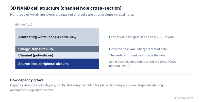
3D NAND is NAND flash memory whose cells are stacked vertically in many layers rather than arranged in one plane. Each cell is formed where a horizontal word-line layer crosses a vertical channel, and a column of cells forms one NAND string. Adding layers raises capacity without shrinking the cell, which planar NAND could no longer do.
Also called: 3D NAND, vertical NAND, V-NAND, BiCS FLASH
Diagram
Why NAND went vertical
Planar NAND gained capacity by shrinking the cell. Below about 15 nm this broke down: neighbouring cells disturbed each other, each cell held too few electrons to tell levels apart, and endurance fell. Building the array vertically let manufacturers relax the cell size again and grow capacity by adding layers. Samsung began volume production in 2013, and all major makers now ship 3D NAND with well over 200 layers.
How the structure is made
Most designs start by depositing alternating layers of silicon oxide and silicon nitride, hundreds of films in total. Channel holes are then etched through the entire stack in one step, with aspect ratios well above 50:1. The hole walls are lined with a blocking oxide, a silicon nitride charge-trap film and a tunnel oxide, and a thin polysilicon channel is formed inside. In a replacement-gate flow, the sacrificial nitride layers are later removed through slits and refilled with tungsten to make the word lines.
Each word-line layer acts as the gate of one cell in every string, so a stack of word lines along one hole is one string. Staircase contacts are etched at the array edge so that each layer can be wired out. When the stack becomes too tall to etch at once, it is built in two or more decks with holes joined between them.
Charge trap, floating gate and CMOS under array
Most 3D NAND stores charge in the nitride charge-trap film, where it stays at its trap site and interferes little with neighbours. Some products have used a floating-gate cell instead. To save die area, the peripheral circuits that drive the array are increasingly placed underneath it (CMOS under array), or built on a separate wafer and bonded to the array wafer. As in planar NAND, each cell can store one to four bits (SLC to QLC).
Japanese companies involved
- Kioxia and its partner Western Digital (now Sandisk) make 3D NAND, called BiCS FLASH, at Yokkaichi in Mie and Kitakami in Iwate. Toshiba, Kioxia's predecessor, proposed the BiCS vertical-string concept in 2007.
- Tokyo Electron and Kokusai Electric supply etch and deposition equipment used to build the tall oxide-nitride stacks and channel holes.
- Tokyo Electron (TEL) · Coat/develop, etch and deposition equipment
- Kokusai Electric · Batch deposition, diffusion and ALD equipment
- Kioxia · NAND flash memory and SSDs
FAQ
Does more layers always mean more capacity?
Capacity per die depends on layers, cell size in the plane, bits per cell and the die area used by peripheral circuits. More layers is the main driver, but makers also shrink the hole pitch, use CMOS under array and move from TLC to QLC.
What limits how many layers can be stacked?
Etching uniform holes through a very tall stack, depositing hundreds of films without stress or thickness drift, and the cost of the extra process time per wafer. Splitting the stack into decks and thinning each layer are the main ways around these limits.
Is 3D NAND the same as 3D DRAM or HBM?
No. 3D NAND stacks cells on one die in a single process flow. HBM stacks separate DRAM dies connected by through-silicon vias. 3D DRAM, which stacks DRAM cells monolithically like 3D NAND, is still in development.
Comparisons
Related pages
Sources
Last updated: November 2, 2026