Hybrid Bonding
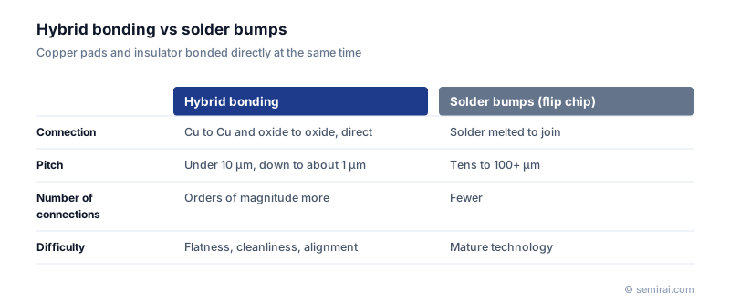
Hybrid bonding is a method of stacking dies or wafers in which the copper pads and the surrounding silicon oxide of two surfaces are bonded directly at the same time, with no solder bumps. Because there is no solder to spread, the connection pitch can shrink to a few micrometres or less, giving far denser, shorter and lower-power vertical connections.
Also called: Cu-Cu hybrid bonding, direct bond interconnect (DBI)
Diagram
How the bond is made
Both surfaces are first polished by chemical mechanical polishing (CMP) so that the oxide is extremely flat and the copper pads sit very slightly below it. After cleaning and plasma activation, the two surfaces are brought together at room temperature, and the oxide layers bond to each other. A later anneal, typically at a few hundred degrees Celsius, makes the copper expand more than the oxide around it, so the pads press together and form a metal bond.
The process is very sensitive to particles, surface roughness and copper recess. A single particle can leave an unbonded area much larger than itself, so hybrid bonding is done in front-end-class cleanrooms with front-end-class CMP and cleaning tools.
Wafer-to-wafer and die-to-wafer
In wafer-to-wafer (W2W) bonding two whole wafers are joined. It is fast and accurate, but both wafers must have the same die size, and a bad die on one wafer is bonded to a good one on the other. Stacked CMOS image sensors use this approach.
In die-to-wafer (D2W) bonding, tested known-good dies are placed one by one on a target wafer. This avoids wasting good dies and allows different die sizes, but placement accuracy, throughput and keeping die edges clean are harder. TSMC's SoIC, used for example in AMD's 3D V-Cache, is a D2W hybrid bonding process, and Intel's Foveros Direct uses the same principle. Hybrid bonding is also being evaluated for future, taller HBM stacks.
Japanese companies involved
- Sony Semiconductor Solutions was among the first to use Cu-Cu hybrid bonding in volume production, joining the pixel wafer and logic wafer of its stacked CMOS image sensors.
- Tokyo Electron offers wafer bonding systems, and Japanese CMP and cleaning equipment and materials are used to prepare the bonding surfaces.
- Sony Semiconductor Solutions · CMOS image sensors
- Tokyo Electron (TEL) · Coat/develop, etch and deposition equipment
FAQ
How does hybrid bonding differ from flip chip?
Flip chip connects through solder bumps tens of micrometres wide at pitches of roughly 40-150 µm. Hybrid bonding uses no solder and bonds copper directly at pitches of about 10 µm down to 1 µm, so it can place one or two orders of magnitude more connections in the same area.
Why is CMP so important for hybrid bonding?
The oxide and copper of both surfaces must touch over the whole area. That requires near-atomic flatness and tightly controlled copper dishing, which only CMP can deliver. Poor planarity directly causes bonding voids and failed connections.
Comparisons
Related pages
- HBM4 (High Bandwidth Memory 4)
- CoWoS (Chip on Wafer on Substrate)
- Backgrinder (Back Grinding Equipment)
- Wafer Thinning
- Temporary Bonding and Debonding (TBDB)
- CMOS under Array (CUA) and CMOS Bonded Array (CBA)
- Copper Recess (for Hybrid Bonding)
- CMOS Image Sensor (CIS)
- Hybrid bonding equipment
- Tokyo Electron (TEL) Synapse™ ZF
- Tokyo Electron (TEL) Ulucus™ L
- Tokyo Electron (TEL) Ulucus™ LX
- Shibaura Mechatronics HSM-1000
Sources
Last updated: November 13, 2026