Angstrom Era
The angstrom era is an industry term for the period in which process node names move from nanometres to angstroms (1 angstrom = 0.1 nm). It became widely used after Intel's 2021 roadmap introduced names such as Intel 20A and Intel 18A. As with nanometre names, the numbers are generation labels, not physical dimensions.
Also called: angstrom nodes, Intel 18A, A16
Diagram
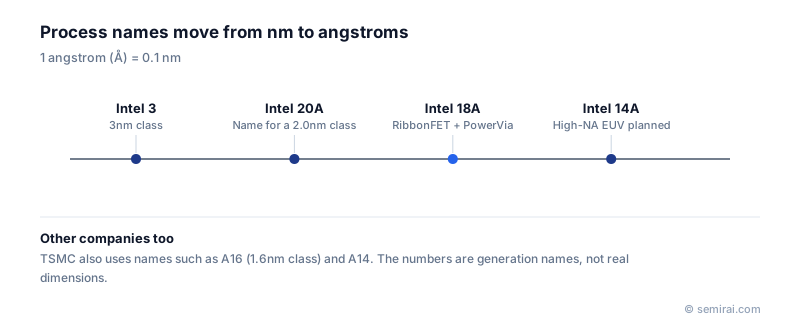
The naming change
In July 2021 Intel renamed its roadmap and introduced Intel 20A and Intel 18A as the generations after Intel 3, later adding Intel 14A. In 2024 Intel dropped 20A as a product node and concentrated on 18A, which combines RibbonFET gate-all-around transistors with PowerVia backside power delivery. TSMC uses similar labels for its generations after N2: A16, which adds backside power through its Super Power Rail, and A14. Samsung has announced a 1.4nm-class process as well.
The new labels say little about real dimensions. What they mark is a set of structural changes that arrive together: gate-all-around transistors, power delivery from the back of the wafer and new interconnect materials.
What makes the angstrom era hard
Patterning is the first challenge. High-NA EUV lithography, with a numerical aperture of 0.55, is being introduced for the finest layers, and edge placement error, the combined error in where pattern edges land, must be held to a few nanometres. Atomic layer deposition (ALD) and atomic layer etching (ALE) are needed to build structures one layer of atoms at a time, and metrology must measure features hidden inside three-dimensional stacks.
Beyond nanosheets, researchers at imec and the major manufacturers are developing forksheet and CFET transistors and air-gap insulation between wires, to keep density rising.
Japanese companies involved
- Rapidus is targeting 2nm first and has said it plans to follow with finer generations.
- Tokyo Electron supplies deposition, etch and coater/developer equipment whose precision requirements rise with each of these generations.
- Rapidus · Leading-edge logic foundry (2 nm, in development)
- Tokyo Electron (TEL) · Coat/develop, etch and deposition equipment
FAQ
Is Intel 18A the same as 1.8 nm?
Only as a name. 18A means 18 angstroms, but nothing on the chip measures 1.8 nm. Intel chose the label to signal its place in the generation sequence relative to competitors.
Why did manufacturers switch to angstrom names?
Counting down below 2 in nanometres would have meant decimal names. Angstroms let companies keep whole numbers and mark a new phase of scaling, but the label is a marketing and roadmap convention rather than a measurement.
Related pages
Sources
Last updated: November 2, 2026