Nanosheet Transistor
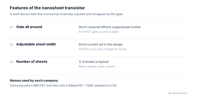
A nanosheet transistor is a form of gate-all-around (GAA) field-effect transistor in which the channel is a stack of thin, horizontal semiconductor sheets, each surrounded on all sides by the gate. It replaces the single vertical fin of a FinFET, and can be thought of as a nanowire transistor widened into a flat ribbon. Samsung calls its version MBCFET and Intel calls its version RibbonFET.
Also called: nanosheet FET, MBCFET, RibbonFET
Diagram
Why sheets instead of fins
Because the gate surrounds every sheet, it controls the channel more tightly than a FinFET gate, which covers only three sides of a fin. Short-channel effects are reduced, so leakage stays low while the on-current stays high. Stacking several sheets, typically three or four, multiplies the current available from the same footprint.
The sheet width is a design variable. In a FinFET, drive strength can only be changed by adding whole fins. In a nanosheet process, wide sheets can be used for high-performance logic and narrow sheets for SRAM or low-power cells, all in the same process.
How nanosheets are made
The process starts with alternating epitaxial layers of silicon and silicon-germanium (SiGe). After patterning, the SiGe is removed by a highly selective etch, leaving silicon sheets a few nanometres thick suspended between the source and drain. Before that, the ends of the SiGe layers are recessed and filled with insulating inner spacers to separate gate and source/drain. The gaps are then coated with a high-k dielectric and metal gate by atomic layer deposition (ALD). Uniform sheet stacking, damage-free inner spacers and void-free gate fill largely decide yield.
Samsung began production with nanosheets on its 3nm process in 2022, TSMC started volume production of N2 nanosheets in the fourth quarter of 2025, and Intel uses RibbonFET in Intel 18A.
Japanese companies involved
- Rapidus is developing a 2nm nanosheet process at its pilot line in Chitose, Hokkaido.
- Tokyo Electron supplies etch and deposition equipment used for steps such as selective SiGe removal and gate-stack formation.
- Rapidus · Leading-edge logic foundry (2 nm, in development)
- Tokyo Electron (TEL) · Coat/develop, etch and deposition equipment
FAQ
What comes after the nanosheet transistor?
Two successors are under study. The forksheet places n-type and p-type sheets on either side of a thin dielectric wall so the two can sit closer together. CFET (complementary FET) stacks n-type and p-type devices vertically, roughly halving the footprint of a logic cell.
How is a nanosheet different from a nanowire?
Both are gate-all-around channels. A nanowire is narrow in both directions, while a nanosheet is wide and thin. The wider sheet carries more current per stack, which is why manufacturers chose sheets for production.
Comparisons
Related pages
Sources
Last updated: November 2, 2026