2nm Process (2nm Node)
The 2nm process is the logic manufacturing generation that follows 3nm. As with earlier nodes the number is a name, not a physical gate length. Representative processes are TSMC N2, which entered volume production in 2025, Samsung SF2 and Intel 18A. The generation is a major turning point because the transistor itself changes from FinFET to gate-all-around (GAA) nanosheets.
Also called: 2 nm node, N2, SF2
Diagram
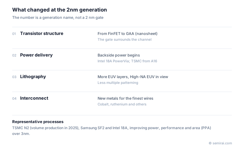
What changes at 2nm
The headline change is the nanosheet transistor. Instead of a vertical fin, the channel is a stack of thin horizontal silicon sheets, each wrapped by the gate on every side. This improves control of leakage and lets designers vary sheet width to trade speed against power. Samsung calls its version MBCFET; Intel calls its version RibbonFET.
Power delivery is changing too. Intel 18A introduces PowerVia, which moves the power network to the back of the wafer. TSMC keeps front-side power for N2 and plans to add backside power, called Super Power Rail, in its later A16 process.
Lithography and interconnect
More layers are printed with EUV lithography, and high-NA EUV scanners with a numerical aperture of 0.55 are being evaluated for the most critical layers to reduce multiple patterning. In the interconnect, copper becomes more resistive as lines narrow, because the barrier liner takes up a larger share of the line and electrons scatter at surfaces and grain boundaries. Alternatives such as ruthenium and cobalt are being studied or used for the finest local wiring.
TSMC states that N2 offers 10-15% more speed at the same power, or 25-30% lower power at the same speed, compared with its N3E process.
Japanese companies involved
- Rapidus is building a 2nm GAA process at its IIM-1 fab in Chitose, Hokkaido, with technology developed together with IBM, and aims to start volume production in 2027.
- Tokyo Electron supplies coater/developers, etch and deposition tools used in 2nm-class fabs.
- Rapidus · Leading-edge logic foundry (2 nm, in development)
- Tokyo Electron (TEL) · Coat/develop, etch and deposition equipment
FAQ
Is a 2nm transistor really 2 nanometres?
No. The gate length and pitches are many times larger. The name continues the tradition of shrinking the label with each generation, and companies apply it differently, so density figures are a better basis for comparison.
Which chips use 2nm processes?
The first products are high-end smartphone and PC processors and AI accelerators, whose makers need the best performance per watt and can afford the high design and wafer costs of a new node.
Related pages
Sources
Last updated: November 2, 2026