CMOS Image Sensor (CIS)
A CMOS image sensor (CIS) is a solid-state imaging device that converts light into electrical signals using CMOS (complementary metal-oxide-semiconductor) technology. It is the image sensor in almost every smartphone, digital camera, car camera, security camera and medical endoscope, and has largely replaced the older CCD sensor. Sony Semiconductor Solutions is the largest maker.
Also called: CIS, CMOS sensor
Diagram
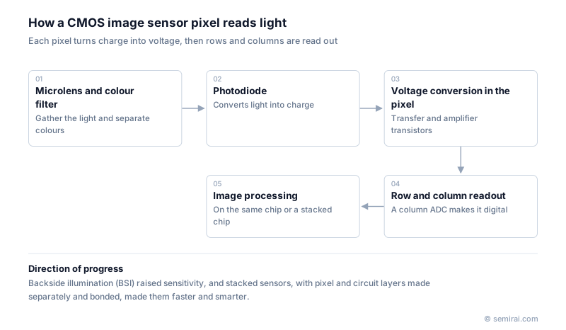
How a CMOS pixel works
The sensor is a two-dimensional array of pixels. Each pixel has a microlens and a colour filter on top, a photodiode that converts light into charge, and a few transistors: a transfer transistor that moves the charge to a sensing node, a reset transistor, and an amplifier transistor that turns the charge into a voltage. Rows are selected one at a time, and column circuits, usually with an analog-to-digital converter (ADC) per column, read the values out in parallel.
Because each pixel amplifies its own signal and the readout is parallel, CMOS sensors are fast and use little power, and the timing, conversion and image processing circuits can sit on the same chip.
BSI and stacked sensors
In a front-illuminated sensor, light must pass between the metal wiring to reach the photodiode. Backside illumination (BSI) flips the wafer and thins it, so light enters from the back and the wiring no longer blocks it, which greatly improves sensitivity in small pixels.
Sony went further with the stacked sensor, introduced as Exmor RS in 2012. The pixel array and the logic circuits are made on separate wafers, each with a process suited to it, and then bonded together, first using through-silicon vias and later direct copper-to-copper hybrid bonding. This allows faster readout and more on-chip processing. Wafer bonding, thinning and fine patterning are therefore central to CIS manufacturing. Automotive sensors must also meet automotive quality and functional safety requirements.
Japanese companies involved
- Sony Semiconductor Solutions designs and makes CMOS image sensors, with production in Kyushu including Kumamoto and Nagasaki.
- Hamamatsu Photonics makes CMOS and other image sensors for scientific, medical and industrial instruments.
- Sony Semiconductor Solutions · CMOS image sensors
- Hamamatsu Photonics · Failure analysis, process monitoring and static elimination equipment
FAQ
What is the difference between a CMOS sensor and a CCD?
A CCD shifts each pixel's charge across the chip to a single output amplifier, while a CMOS sensor converts charge to voltage inside each pixel and reads rows in parallel. CMOS is faster, uses less power and integrates processing on chip, which is why it took over most markets.
What is a global shutter?
Most CMOS sensors read rows one after another (rolling shutter), which can distort fast-moving objects. A global shutter sensor captures all pixels at the same instant by adding storage in each pixel, which is valuable in machine vision and automotive uses.
Related pages
Sources
Last updated: November 2, 2026