EUV Lithography Equipment (EUV Scanner)
EUV lithography equipment is the exposure tool that prints circuit patterns with extreme ultraviolet (EUV) light at a wavelength of 13.5 nm, about one fourteenth of the 193 nm used in ArF immersion lithography. The short wavelength lets the finest layers of leading-edge logic and DRAM be printed in a single exposure instead of several, but it requires a plasma light source and all-mirror optics in vacuum.
Also called: EUV scanner, EUV exposure tool, EUV lithography system
Diagram
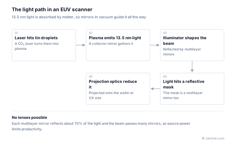
How an EUV scanner works
The light source fires a high-power CO₂ laser at tiny droplets of molten tin, many thousands of times per second. The tin becomes a hot plasma that emits 13.5 nm light, and a collector mirror gathers it. This laser-produced plasma (LPP) source works on a completely different principle from the excimer lasers of DUV tools.
EUV light is absorbed by air, glass and almost every other material, so no lenses can be used and the light path is kept in vacuum. The beam is shaped by an illuminator, reflected from a mask that is itself a mirror, and reduced four times by the projection optics onto the wafer. Each mirror is coated with dozens of alternating molybdenum and silicon layers and reflects only about 70% of the light, so much of the source power is lost along the way and source power directly limits throughput.
Why chipmakers use it, and what is hard
Before EUV, the smallest pitches had to be split across two or four ArF immersion exposures, each with its own deposition and etch steps. One EUV exposure replaces several of those steps, shortens the process flow and avoids the overlay errors between split patterns. EUV is therefore used for the most critical layers at 7 nm-class logic nodes and below and in recent DRAM generations, while DUV tools still print most other layers.
The hard parts sit across the ecosystem: resists must balance sensitivity, resolution and roughness against random photon effects; pellicles must survive the heat while letting the light through; masks need defect-free multilayer blanks and inspection at the EUV wavelength. High-NA EUV raises the numerical aperture from 0.33 to 0.55 for finer resolution.
Japanese companies involved
- Lasertec makes actinic inspection systems that check EUV mask blanks and masks using light at the EUV wavelength.
- HOYA and AGC make EUV mask blanks, Mitsui Chemicals makes EUV pellicles, and JSR, Tokyo Ohka Kogyo (TOK) and Shin-Etsu Chemical make EUV resists.
- Rapidus has installed EUV scanners at its pilot line in Chitose, Hokkaido, for its planned 2 nm logic production.
- Lasertec · EUV mask and mask blank inspection
- HOYA · Mask blanks (including EUV) and photomasks
- AGC · EUV mask blanks and glass materials
- Mitsui Chemicals · EUV pellicles and wafer protection tapes
- JSR · Photoresists and semiconductor materials
- Tokyo Ohka Kogyo (TOK) · Photoresists and high-purity process chemicals
- Shin-Etsu Chemical · Silicon wafers, photoresists and photomask blanks
FAQ
Who makes EUV lithography equipment?
Only ASML of the Netherlands supplies production EUV scanners. It integrates subsystems from a large supply chain, notably the optics from Carl Zeiss and the CO₂ drive laser from Trumpf.
Is the inside of an EUV scanner a perfect vacuum?
Not entirely. The light path is kept at very low pressure, but a small amount of hydrogen gas is deliberately present in the source and around the optics. It slows tin debris and helps keep the mirrors clean, and it absorbs little EUV light.
Does EUV completely replace DUV lithography?
No. Even in the most advanced chips, only a minority of layers are exposed with EUV. KrF and ArF tools are cheaper per exposure and print the many less critical layers.
Related pages
Sources
Last updated: November 2, 2026