CMOS (Complementary Metal-Oxide-Semiconductor)
CMOS (complementary metal-oxide-semiconductor) is a way of building logic circuits from pairs of n-channel and p-channel MOSFETs that switch in opposition. For any steady input only one of the pair conducts, so almost no current flows from supply to ground, which is why CMOS is the basis of virtually every modern processor, memory and SoC.
Also called: complementary MOS
Diagram
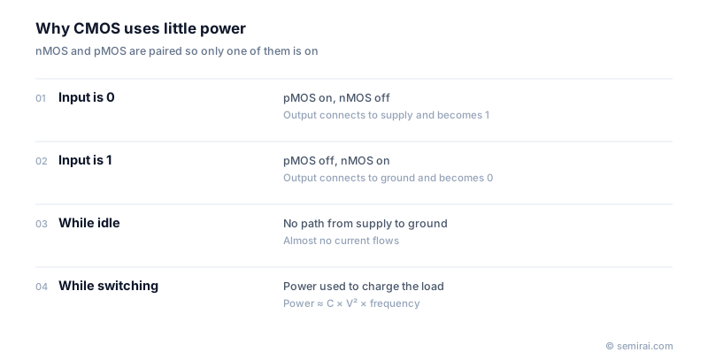
How the CMOS inverter works
The simplest CMOS gate is the inverter: a pMOS transistor connects the output to the supply voltage and an nMOS transistor connects it to ground. A high input turns the nMOS on and the pMOS off, pulling the output low; a low input does the opposite. NAND, NOR and more complex gates are built the same way, with a pull-up network of pMOS and a pull-down network of nMOS.
Power is consumed mainly when the output switches and the load capacitance is charged or discharged. This dynamic power is roughly proportional to capacitance times the square of the supply voltage times the switching frequency, which is why lowering the voltage has been the most effective way to save energy. The output swings fully from ground to supply, giving wide noise margins.
From planar CMOS to FinFET and GAA
CMOS replaced bipolar and nMOS-only logic during the 1980s because it used far less power and could be packed more densely. It then followed Moore's law for decades. As transistors shrank, the planar device was replaced by the FinFET and now by gate-all-around (GAA) nanosheets, but every one of these generations is still CMOS: complementary n- and p-type devices switching in pairs.
In manufacturing, n-wells and p-wells are formed so both transistor types can sit on one wafer (twin-well CMOS), and shallow trench isolation separates them. The adjacent wells form a parasitic thyristor that can latch up and short the supply, so layouts use guard rings and well contacts to prevent it. High-k metal gates and multiple threshold-voltage options are standard parts of today's CMOS processes.
Japanese companies involved
- Sony Semiconductor Solutions makes CMOS image sensors, in which the photodiodes and readout circuits are built with CMOS processes on the same chip.
- Sony Semiconductor Solutions · CMOS image sensors
FAQ
Does CMOS really draw no current when idle?
Not quite. Ideal CMOS draws no static current, but real transistors leak. Subthreshold leakage through transistors that are off and tunnelling through thin gate dielectrics grew with each node, and in advanced chips leakage is a significant part of total power.
Is the CMOS in CMOS image sensor the same thing?
Yes. A CMOS image sensor is made with a CMOS process, so the pixel photodiodes and the amplifiers and converters that read them can share one chip. That integration gave CMOS sensors lower power and faster readout than CCDs, and they now dominate cameras.
What does the CMOS setting in a PC refer to?
Older PCs stored BIOS settings in a small battery-backed memory made with CMOS technology, so the settings memory itself came to be called the CMOS. It refers to the same technology, used in one particular chip.
Related pages
Sources
Last updated: November 2, 2026