Backside Interconnect
Backside interconnect is the collective term for technologies that form metal wiring on the back side of a chip's silicon substrate. Conventional chips have all their wiring on the front, above the transistors. Adding wiring on the back lets connections reach the transistors from both sides, improving wiring density and power quality at the same time.
Also called: backside metallization, backside wiring
Diagram
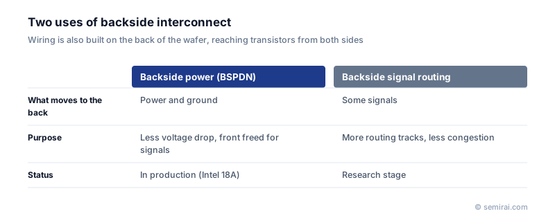
Two uses of the back side
The first and more mature use is backside power delivery (BSPDN), which moves the power and ground network to the back of the wafer. This reduces voltage drop and frees front-side layers for signals. Intel's PowerVia in Intel 18A is in production, and TSMC plans its Super Power Rail for A16.
The second use is backside signal routing, in which some signal nets, for example long or critical connections, are also routed on the back to relieve congestion on the front. This is still at the research stage, studied by imec among others, and needs design tools that can place and route on both sides.
What the process requires
The wafer is temporarily or permanently bonded to a carrier, often by direct oxide-to-oxide or copper-to-copper bonding, and the original substrate is thinned by grinding, CMP and etching. Nano-through-silicon vias are then etched from the back to connect to the front-side devices, and liners and metals are deposited by ALD and PVD. Each step must be aligned to structures that are now hidden on the other side of the wafer, and wafer distortion after bonding must be kept small enough for lithography to overlay correctly.
Japanese companies involved
- DISCO and Tokyo Seimitsu supply wafer grinding and polishing equipment of the kind used for the thinning step.
- Tokyo Electron develops etch, deposition and wafer bonding equipment for advanced logic and 3D integration.
- Tokyo Seimitsu (ACCRETECH) · Wafer probers, dicing and grinding machines, metrology
- DISCO · Dicing, grinding and polishing equipment
FAQ
Is backside interconnect the same as BSPDN?
BSPDN is one application of it. Backside interconnect is the broader idea of wiring on the back of the chip, which includes power delivery today and possibly signal routing in the future.
Does backside wiring make chips hotter?
It can make heat removal harder. The thick silicon substrate that used to spread heat is ground away and replaced by wiring and a bonded carrier, so thermal paths have to be designed carefully, especially for high-power processors.
Related pages
Sources
Last updated: November 2, 2026