Backside Power Delivery Network (BSPDN)
A backside power delivery network (BSPDN) is a chip architecture in which the power supply wiring (VDD and ground) is built on the back side of the wafer, leaving the front-side interconnect for signals only. In conventional chips power and signal wires share the same metal layers, which causes routing congestion and voltage drop. Moving power to the back addresses both problems.
Also called: backside power delivery, PowerVia, Super Power Rail
Diagram
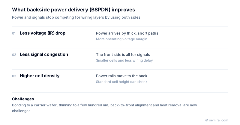
What BSPDN improves
In a front-side design, current from the package must pass down through every metal layer, from the thick top layers to the thin wires near the transistors, before it reaches them. The resistance along that path causes a voltage drop known as IR drop. On the back of the wafer, the power wires can be short and thick and connect almost directly to the transistors, so the drop is much smaller and the supply more stable.
Freeing the front-side layers from power rails also eases signal routing. Standard cells no longer need space for power rails, so they can be made smaller, raising logic density. High-power chips such as GPUs, CPUs and AI accelerators benefit most.
How it is made
After the transistors and front-side interconnect are completed, the wafer is bonded face-down to a carrier wafer. The original substrate is then ground and polished away until only a very thin layer remains, and nano-scale vias are formed from the back to reach the transistor level. The power network is built on this exposed surface. Bonding, extreme thinning, back-to-front alignment and heat removal are the main new challenges.
Intel was first to put it into a product process, as PowerVia in Intel 18A, after showing it on a test chip called Blue Sky Creek in 2023. TSMC plans to introduce backside power, which it calls Super Power Rail, in its A16 process.
Japanese companies involved
- DISCO and Tokyo Seimitsu make grinding and polishing equipment of the kind used to thin wafers, a step that backside power delivery makes far more demanding.
- Tokyo Electron supplies etch and deposition equipment used to form the backside vias and wiring.
- Tokyo Seimitsu (ACCRETECH) · Wafer probers, dicing and grinding machines, metrology
- DISCO · Dicing, grinding and polishing equipment
FAQ
What is IR drop?
IR drop is the voltage lost as current (I) flows through the resistance (R) of the power wiring. If the voltage at the transistors falls too far, circuits slow down or fail, so designers must leave margin. Reducing IR drop lets chips run at lower supply voltage or higher clock speed.
What is a buried power rail?
A buried power rail places the power rail below the transistors, inside the substrate, instead of in the first metal layer. It is a related approach that can be combined with backside power delivery, which then connects to the buried rails from the back.
Related pages
Sources
Last updated: November 1, 2026