Fermi Level
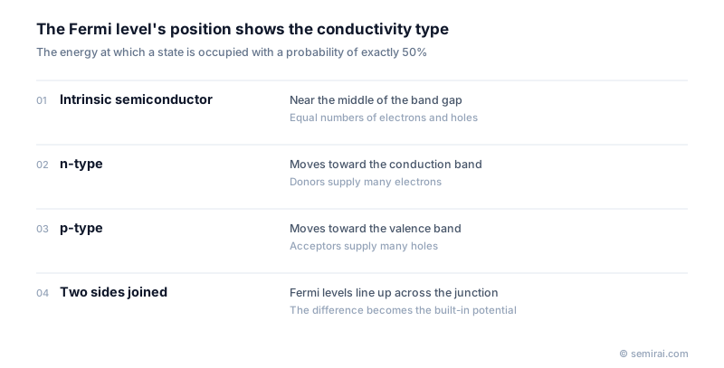
The Fermi level (E_F) is the energy at which an electron state would be occupied with a probability of exactly one half in thermal equilibrium. On a band diagram it is the reference line that shows how full the bands are: its position relative to the conduction and valence bands tells whether a semiconductor is n-type, p-type or intrinsic, and how many carriers it holds.
Also called: E_F, Fermi energy, electrochemical potential
Diagram
The Fermi-Dirac distribution
Electrons fill available states according to the Fermi-Dirac distribution. At absolute zero every state below E_F is full and every state above it is empty; at higher temperatures the step softens over a range of a few kT (kT is about 0.026 eV at room temperature). In a metal, E_F lies inside a band, so at absolute zero it is the energy of the highest occupied state.
In a semiconductor, E_F normally lies inside the band gap, where there are no states at all, so the 50% occupancy is a mathematical reference rather than a real level. What matters is its distance to the band edges: the electron concentration falls exponentially as the gap between E_F and the conduction band grows, and the hole concentration likewise with distance from the valence band.
Position in intrinsic, n-type and p-type material
In intrinsic silicon E_F sits close to the middle of the gap. Adding donors moves it towards the conduction band: at room temperature each tenfold increase in electron concentration raises it by about 60 meV. Acceptors move it towards the valence band in the same way. In very heavily doped (degenerate) material E_F enters the band itself, and the semiconductor behaves almost like a metal. As temperature rises, intrinsic carriers grow and E_F drifts back towards mid-gap.
Why the Fermi level is flat in equilibrium
When two materials touch, electrons flow from the side with the higher E_F until the Fermi levels line up; with no applied voltage, E_F is flat through the whole structure. In a pn junction the bands bend to make this possible, and the original difference between the two Fermi levels becomes the built-in potential. The same principle explains the barrier at a metal-semiconductor (Schottky) contact and band bending in a MOS capacitor.
Under bias or illumination, electrons and holes are no longer in equilibrium with each other, and each population is described by its own quasi-Fermi level. Their separation equals the applied voltage in a diode and limits the open-circuit voltage of a solar cell.
FAQ
How is the Fermi level related to the work function?
The work function is the energy needed to take an electron from the Fermi level to the vacuum just outside the surface. Choosing gate metals with suitable work functions is one way the threshold voltage of nMOS and pMOS transistors is set.
What is Fermi-level pinning?
At many metal-semiconductor interfaces, interface states fix the semiconductor's Fermi level near a certain energy regardless of the metal used. The barrier height then barely depends on the metal's work function, which makes low-resistance contacts harder to design.
Are the Fermi level and the Fermi energy the same thing?
Often used interchangeably, but in metals 'Fermi energy' usually means the absolute-zero value measured from the bottom of the band, while 'Fermi level' means the electrochemical potential of electrons at any temperature.
Related pages
Sources
Last updated: November 2, 2026