Heterojunction
A heterojunction is a junction between two different semiconductors grown as one continuous crystal, such as GaAs and AlGaAs, GaN and AlGaN, or Si and SiGe. A junction between p-type and n-type regions of the same material is a homojunction. The prefix hetero comes from the Greek for different.
Also called: hetero junction, heterostructure
Diagram
Band offsets and how they are used
Because the two materials have different bandgaps, the conduction and valence bands step up or down at the interface. These steps, called band offsets, let designers confine electrons or holes to a chosen layer, or make carriers flow easily in one direction and poorly in the other. A homojunction cannot do this.
Good heterojunctions need materials with similar lattice constants, or a strained layer kept thinner than the critical thickness at which dislocations form. They are grown by epitaxy, usually metal-organic chemical vapour deposition (MOCVD) or molecular beam epitaxy (MBE), which can produce interfaces that are abrupt on the atomic scale.
Devices built on heterojunctions
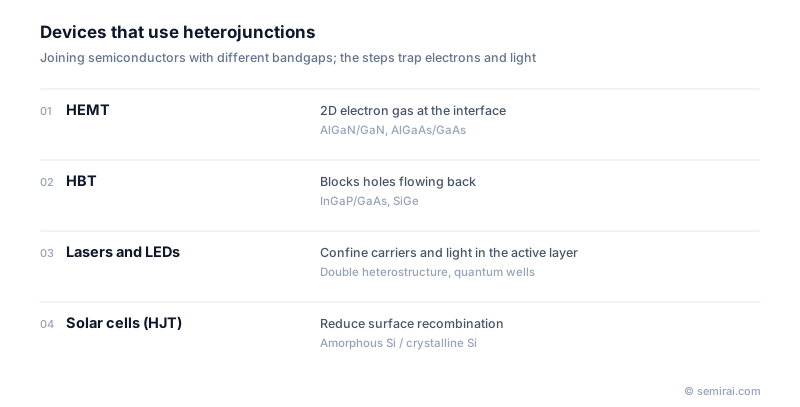
The high electron mobility transistor (HEMT) uses the two-dimensional electron gas that forms at an AlGaAs/GaAs or AlGaN/GaN interface and works at high frequency and high power. The heterojunction bipolar transistor (HBT) uses a wide-bandgap emitter to stop holes flowing back from the base, which raises current gain; InGaP/GaAs HBTs are common in smartphone power amplifiers, and SiGe HBTs are used in RF circuits.
Semiconductor lasers and LEDs use double heterostructures and quantum wells to trap carriers and light in the active layer. Work on these structures was recognised in the 2000 Nobel Prize in Physics, shared by Zhores Alferov and Herbert Kroemer. Heterojunction (HJT) solar cells combine amorphous and crystalline silicon to reduce surface recombination.
Japanese companies involved
- Sumitomo Electric Industries supplies GaAs and InP substrates on which compound semiconductor heterostructures are grown.
- Sumitomo Electric Industries (compound semiconductors) · SiC epitaxial wafers and GaAs and InP substrates
FAQ
What makes heterojunctions hard to manufacture?
Different materials have different atomic spacings and thermal expansion. A poor match creates strain and dislocations at the interface that trap carriers and degrade the device. Growers choose lattice-matched pairs or keep strained layers thin, and control the growth to avoid mixing at the interface.
Is a silicon transistor with a SiGe channel a heterojunction device?
Yes. SiGe on silicon forms a heterojunction with a smaller bandgap and a strained lattice. It is used in SiGe HBTs for high-frequency circuits and in the p-type channels of some advanced CMOS transistors to raise hole mobility.
Related pages
- PN Junction
- Band Gap
- High Electron Mobility Transistor (HEMT)
- Gallium Arsenide (GaAs)
- Gallium Nitride (GaN)
- Lattice Constant
- Epitaxy (Epitaxial Growth)
- Compound Semiconductor
- Compound semiconductor equipment
- MOCVD equipment
- RF semiconductor (GaN/GaAs) equipment
- Canon ANELVA EC7400
- Canon ANELVA EC8100
- EpiQuest MPC6100
- EpiQuest SH series
Sources
Last updated: November 13, 2026