Field-Effect Transistor (FET)
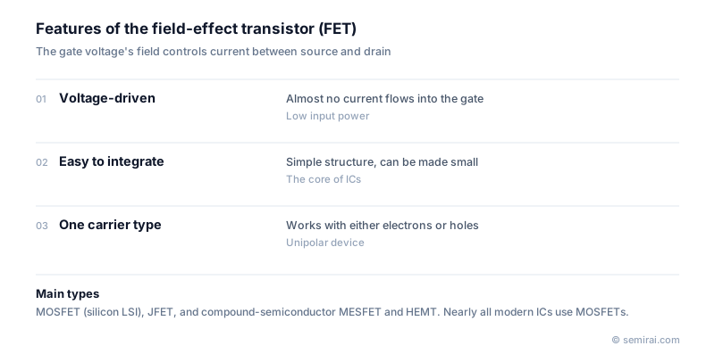
A field-effect transistor (FET) is a semiconductor device in which the electric field created by a voltage on the gate electrode controls the current flowing between source and drain. Because it is driven by voltage rather than current, almost no gate current flows, so it uses little input power and is well suited to integration.
Also called: FET, MOSFET, JFET, HEMT
Diagram
How a FET works
A FET has three terminals: gate, source and drain. Current flows through a channel between source and drain, and the gate voltage changes how many carriers the channel contains, switching it on or off or setting its resistance. In a MOSFET the gate is separated from the channel by a thin insulator, so the input draws practically no current and has very high impedance.
A FET uses only one type of carrier, electrons in n-channel devices and holes in p-channel devices, so it is called a unipolar device. This contrasts with the bipolar transistor, which relies on both carrier types and is controlled by a base current.
Main types
The MOSFET is by far the most important type. Pairing n-channel and p-channel MOSFETs gives CMOS, the basis of almost all digital chips, because a CMOS gate draws current mainly when it switches. As transistors shrank, the planar MOSFET gave way to the FinFET, in which the gate wraps three sides of a fin, and then to gate-all-around (GAA) nanosheet transistors, in which it surrounds the channel completely.
The junction FET (JFET) controls the channel with a pn junction rather than an insulated gate and is used in low-noise analog circuits. In compound semiconductors, the MESFET uses a Schottky gate, and the high electron mobility transistor (HEMT) uses a heterojunction to form a very fast channel; GaAs and GaN HEMTs serve high-frequency and high-power applications. Power MOSFETs in silicon and SiC are the main switches in power electronics.
Japanese companies involved
- ROHM and Toshiba Electronic Devices & Storage make silicon and SiC power MOSFETs, and Renesas Electronics makes power MOSFETs alongside its microcontrollers.
- Toshiba Electronic Devices & Storage · Power MOSFETs, IGBTs and discrete semiconductors
- ROHM · SiC and silicon power devices, analog ICs
- Renesas Electronics · Microcontrollers, automotive SoCs, analog and power chips
FAQ
What does threshold voltage mean?
It is the gate voltage at which the channel starts to conduct significantly. Chipmakers set it by doping and gate materials, and offering several threshold options lets designers trade speed against leakage.
What is the difference between enhancement and depletion mode?
An enhancement-mode FET is off at zero gate voltage and needs a gate voltage to turn on, as in standard CMOS. A depletion-mode FET conducts at zero gate voltage and needs a voltage to turn off, as in many JFETs and GaN HEMTs.
Related pages
Sources
Last updated: November 2, 2026