High Electron Mobility Transistor (HEMT)
A high electron mobility transistor (HEMT) is a field-effect transistor whose channel is a two-dimensional electron gas (2DEG) formed at the interface between two semiconductors with different band gaps. Because the electrons travel away from the dopant atoms that would scatter them, mobility and speed are high. GaAs and InP HEMTs serve microwave receivers, and GaN HEMTs serve base stations, radar and power conversion.
Also called: HEMT, HFET, heterostructure FET, GaN HEMT, pHEMT
Diagram
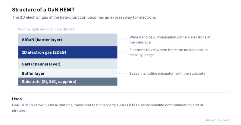
How the electron gas forms
In the original GaAs HEMT, a thin layer of n-doped AlGaAs, which has a wider band gap, sits on undoped GaAs. Electrons from the donors in the AlGaAs drop into the lower-energy GaAs and collect in a sheet only a few nanometres thick at the interface. The ionised donors stay behind in the AlGaAs, so the electrons move with far less impurity scattering than in doped silicon. This technique is called modulation doping.
GaN HEMTs work differently. AlGaN and GaN have strong built-in spontaneous and piezoelectric polarisation, and the difference at the AlGaN/GaN interface draws a dense 2DEG without any intentional doping. A metal Schottky gate on top depletes the channel to switch it. The resulting device is normally on, so power transistors that must be off at zero gate voltage use a p-type GaN gate or other designs.
GaAs, InP and GaN HEMTs
GaAs HEMTs, including pseudomorphic types with an InGaAs channel, have long been used as low-noise amplifiers in satellite receivers, radio astronomy and microwave links. InP-based HEMTs reach the highest frequencies, into the hundreds of gigahertz. GaN HEMTs combine high mobility with GaN's wide band gap and high breakdown field, so they handle far more power: they amplify signals in mobile base stations and radar, usually on SiC substrates that conduct heat well.
GaN HEMTs grown on silicon substrates are now also used as power switches. Their low capacitance lets power supplies switch at high frequency, shrinking chargers and improving data-centre and other power converters.
Japanese companies involved
- The HEMT was invented at Fujitsu Laboratories by Takashi Mimura around 1979-1980.
- Sumitomo Electric Industries developed GaN HEMTs for mobile base station amplifiers and supplies them through its device subsidiary.
- Mitsubishi Electric makes GaN HEMT amplifiers for wireless and satellite communication.
- Sumitomo Electric Industries (compound semiconductors) · SiC epitaxial wafers and GaAs and InP substrates
- Mitsubishi Electric (power devices) · IGBT and SiC power modules, RF and optical devices
FAQ
How is a HEMT different from a silicon MOSFET?
A MOSFET forms its channel in doped silicon under an insulating gate oxide, where electrons scatter off impurities and the rough interface. A HEMT's channel lies in undoped material at a crystal heterojunction, and its gate is usually a Schottky contact. The result is higher mobility and lower noise, but HEMTs need compound semiconductors and are not used for dense digital logic.
Why are RF GaN HEMTs usually built on SiC?
High-power amplifiers produce a lot of heat in a small area. Silicon carbide conducts heat several times better than silicon or sapphire and has a closer lattice match to GaN, so devices run cooler and more reliably. Cost-sensitive power-switching GaN uses silicon substrates instead.
What limits GaN HEMT reliability?
Electrons trapped at the surface or in the buffer can temporarily reduce current after high-voltage stress, an effect called current collapse or dynamic on-resistance. Surface passivation, field plates and buffer design reduce it, and qualifying these effects is a key part of GaN device development.
Comparisons
Related pages
Sources
Last updated: November 2, 2026