Ion Implantation
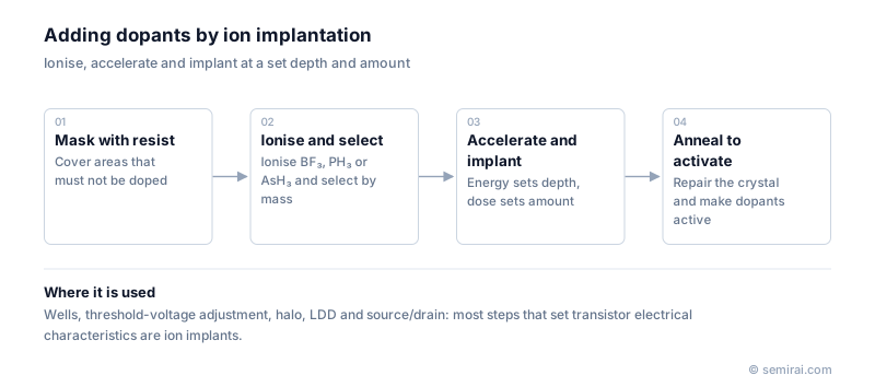
Ion implantation is the process of doping a wafer by ionising dopant atoms such as boron, phosphorus or arsenic, accelerating them and firing them into the silicon so they come to rest at a chosen depth. It forms wells, threshold-voltage adjustments, source/drain regions and many other doped layers, and it is one of the steps that most directly sets transistor characteristics.
Also called: ion implant, implant
Diagram
How an implanter works
An ion source ionises a feed material, usually a gas such as BF₃, PH₃ or AsH₃, in a plasma. The ions are extracted as a beam, and an analyser magnet bends it so that only ions of the wanted mass and charge pass. They are then accelerated to energies from below 1 keV to several MeV and scanned across the wafer, either by sweeping the beam or by moving the wafer mechanically. A Faraday cup measures the beam current so that the number of implanted ions, the dose, can be counted.
Implanters are grouped by what they do best: high-current tools deliver large doses at low energy for source/drain and contact regions, medium-current tools handle precise low and medium doses such as threshold adjustment, and high-energy tools form deep wells and isolation layers.
Energy, dose and the dopant profile
The great advantage over thermal diffusion is that depth and amount are controlled separately. Energy sets the projected range, the mean stopping depth; dose, in atoms per square centimetre, sets how many atoms are added. Ions travelling along open crystal directions penetrate too deep, an effect called channeling, so wafers are often tilted by a few degrees or the surface is first made amorphous.
Implantation knocks silicon atoms out of place and leaves most dopants electrically inactive. An anneal is therefore always needed to repair the crystal and activate the dopants, and its heat must be limited so the profile does not spread.
Where it is used
A CMOS flow contains many implants: n- and p-wells, threshold adjustment, halo or pocket implants against short-channel effects, lightly doped drain extensions and heavily doped source/drain regions. Implantation is also used for hydrogen splitting in SOI wafer production and for doping power devices. In FinFET and gate-all-around transistors, fins shadow each other and side walls are hard to reach, so tilt angles are tightly controlled and plasma doping or in-situ doped epitaxy take over some steps.
Japanese companies involved
- Nissin Ion Equipment makes ion implanters for semiconductor fabs and for flat-panel display production.
- Sumitomo Heavy Industries Ion Technology (SMIT) makes ion implanters, including high-current and high-energy types, for chip fabs.
- Nissin Ion Equipment · Ion implanters
- Sumitomo Heavy Industries Material Solutions (formerly SMIT) · Ion implanters
FAQ
Why did ion implantation replace thermal diffusion for doping?
Diffusion from a surface source couples depth and concentration through temperature and time, and it needs high heat. Implantation sets dose precisely by counting charge, sets depth by energy, works through thin masks of photoresist and runs near room temperature, which suits ever smaller and shallower structures.
What do Axcelis and Applied Materials make in this field?
Both are major makers of ion implanters: Axcelis Technologies with its Purion family and Applied Materials with its VIISta family. Together with the Japanese makers they supply the high-current, medium-current and high-energy tools used in logic, memory and power device fabs.
Comparisons
Related pages
Sources
Last updated: November 2, 2026