N-type and P-type Semiconductor
N-type and p-type semiconductors are the two kinds of doped (extrinsic) semiconductor. N-type material contains donor impurities such as phosphorus or arsenic, so free electrons carry most of the current; p-type material contains acceptors such as boron, so holes do. The letters refer to the negative and positive charge of these majority carriers.
Also called: n-type, p-type, extrinsic semiconductor, doped semiconductor
Diagram
How doping creates electrons and holes
Each silicon atom shares its four valence electrons with four neighbours. A phosphorus atom has five; four join the bonds and the fifth is held so loosely that at room temperature it is almost always free, leaving a fixed positive ion behind. A boron atom has only three, so one bond is missing an electron. A neighbouring electron can hop into that gap, and the vacancy that moves around is a hole, which behaves as a positive carrier.
In n-type material electrons are the majority carriers and holes the minority; in p-type the roles reverse. The majority concentration roughly equals the dopant concentration, typically 10¹⁵ to 10²⁰ cm⁻³ against about 5×10²² silicon atoms per cm³, and the minority concentration falls in proportion. Overall the material stays electrically neutral.
Common dopants
For silicon, phosphorus, arsenic and antimony are donors; boron is the main acceptor, often implanted as BF₂ for shallow junctions. Other materials need other elements: SiC is made n-type with nitrogen and p-type with aluminium, while GaN uses silicon as a donor and magnesium as an acceptor.
How n- and p-regions are made and used
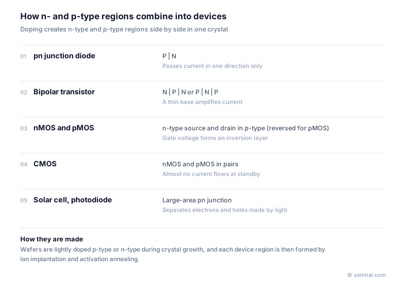
Wafers are lightly doped during crystal growth by adding dopant to the melt. Inside a chip, each region is then formed locally by ion implantation, followed by an activation anneal that moves dopant atoms onto lattice sites and repairs implant damage; older processes used thermal diffusion, and epitaxial layers can be doped as they grow. The dopant profile sets threshold voltage, resistance and breakdown voltage.
Putting the two types side by side makes a pn junction. Three layers (npn or pnp) make a bipolar transistor, and an n-type source and drain in a p-type well, controlled by a gate, make an nMOS transistor. CMOS pairs nMOS and pMOS transistors.
Japanese companies involved
- Sumitomo Heavy Industries Material Solutions (formerly SMIT) and Nissin Ion Equipment make ion implanters that place donors and acceptors into silicon and SiC wafers.
- Kokusai Electric makes batch furnaces used for diffusion and annealing steps.
- Sumitomo Heavy Industries Material Solutions (formerly SMIT) · Ion implanters
- Nissin Ion Equipment · Ion implanters
- Kokusai Electric · Batch deposition, diffusion and ALD equipment
FAQ
Is n-type material negatively charged?
No. Every free electron in n-type material is balanced by a positively charged donor ion fixed in the lattice, so the material is neutral. 'N' only describes which carrier is in the majority.
What happens if both donors and acceptors are present?
They compensate each other: electrons from donors fill the acceptors' empty bonds. The type is set by whichever is more numerous, and the carrier concentration by the difference. Counter-doping is used deliberately, for example to form a p-type well inside an n-type region.
Why was p-type GaN difficult to make?
The magnesium acceptor in GaN lies deep in the band gap and is passivated by hydrogen during growth, so as-grown layers barely conducted. In 1989 Isamu Akasaki and Hiroshi Amano activated it with electron-beam irradiation, and Shuji Nakamura later showed that annealing in nitrogen works, which opened the way to blue LEDs.
Related pages
Sources
Last updated: November 2, 2026