Front-End Equipment
Front-end equipment is the collective term for the machines used in the front-end process, where transistors and multilevel interconnects are built on silicon wafers. It covers both FEOL and BEOL steps and includes lithography, coat and develop, etch, deposition, cleaning, CMP, ion implantation, thermal processing, inspection and metrology tools.
Also called: front-end semiconductor equipment, wafer fab equipment, WFE
Diagram
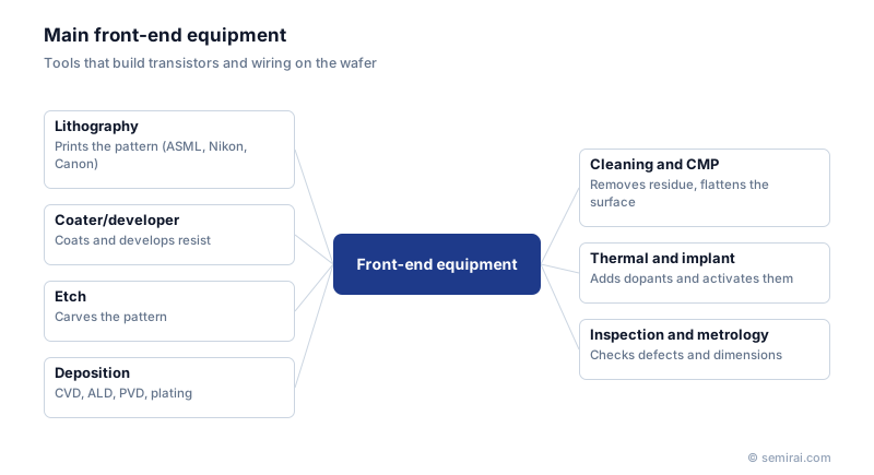
The main equipment categories
Lithography scanners transfer the circuit pattern from a photomask to a resist-coated wafer, using deep ultraviolet (DUV) or extreme ultraviolet (EUV) light. Coater/developers apply the photoresist before exposure and develop it afterwards. Etch tools then use the resist pattern as a mask to remove silicon, dielectric or metal selectively, while deposition tools add thin films by chemical vapour deposition (CVD), physical vapour deposition (PVD), atomic layer deposition (ALD) or electroplating.
Cleaning tools remove particles and residues between steps, and chemical mechanical polishing (CMP) flattens the surface so the next layer can be patterned. Ion implanters introduce dopants and anneal furnaces or lamps activate them. Inspection tools look for pattern defects and particles, and metrology tools measure film thickness, critical dimension (CD) and overlay between layers.
Why the tools work as one system
A leading-edge chip passes through many hundreds of front-end steps, and the same sequence of deposition, lithography, etch and cleaning is repeated for each layer. A small drift in any one tool shows up later as lost yield, so uptime, precision and throughput all feed directly into the cost of a finished wafer.
Fabs therefore collect process data from every tool and use advanced process control (APC) to adjust recipes from lot to lot. Metrology results after one step are fed back to the tool that ran it, or forward to the next one, so that the whole line behaves as a controlled system rather than a set of separate machines.
Japanese companies involved
- Tokyo Electron supplies coater/developers, etch, deposition, cleaning and wafer probing equipment, and SCREEN Holdings is a major maker of wafer cleaning systems.
- Nikon and Canon build DUV lithography systems, and Kokusai Electric makes batch furnaces used for deposition, oxidation and ALD.
- Hitachi High-Tech makes CD-SEMs for measuring pattern dimensions as well as etch systems, and Lasertec specialises in inspection of EUV masks and mask blanks.
- Nikon · ArF, KrF and i-line lithography systems
- Canon · Lithography steppers and nanoimprint lithography
- Kokusai Electric · Batch deposition, diffusion and ALD equipment
- Lasertec · EUV mask and mask blank inspection
- Tokyo Electron (TEL) · Coat/develop, etch and deposition equipment
- Hitachi High-Tech · CD-SEM metrology, defect inspection and etch systems
- SCREEN Holdings · Wafer cleaning, coat/develop and inspection equipment
FAQ
Does front-end equipment include BEOL tools?
Yes. In the equipment business, front end means everything done to the wafer inside the fab, including the interconnect (BEOL) layers. Back-end equipment starts after the wafer is finished: probing, grinding, dicing, bonding, molding and final test.
Which front-end steps are the most expensive?
Lithography carries the highest cost per tool, especially EUV scanners. Etch and deposition, however, are used many more times per wafer, so together they account for a large share of the equipment in a modern fab.
What is the difference between inspection and metrology?
Inspection searches the wafer for things that should not be there, such as particles, scratches or bridged lines. Metrology measures things that should be there, such as film thickness, line width or overlay, and checks that they are within specification.
Comparisons
Related pages
Sources
Last updated: November 1, 2026