Schottky Junction (Schottky Barrier)
A Schottky junction is a rectifying contact between a metal and a semiconductor, in which an energy barrier at the interface (the Schottky barrier) lets current pass easily in one direction only. It is named after the German physicist Walter Schottky, who explained it around 1938, and is the counterpart of an ohmic contact, which conducts both ways.
Also called: Schottky contact, metal-semiconductor junction
Diagram
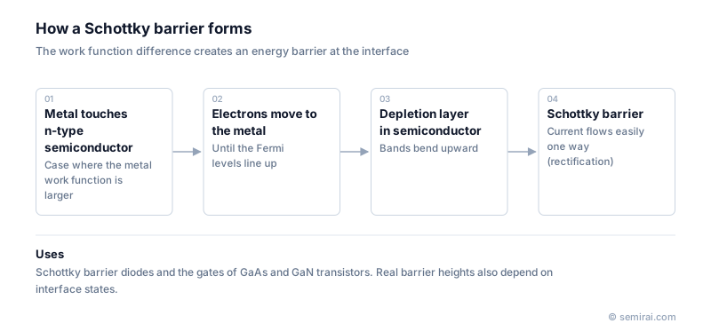
How the barrier forms and conducts
When a metal touches an n-type semiconductor, electrons move until the Fermi levels line up, leaving a depletion region in the semiconductor and bending its bands upward. In the ideal case the barrier height is the difference between the metal work function and the semiconductor electron affinity (the Schottky-Mott rule). In real silicon and GaAs, interface states pin the Fermi level, so changing the metal changes the barrier less than theory predicts.
Under forward bias, electrons from the semiconductor cross the barrier into the metal by thermionic emission; under reverse bias very little current flows. Because only majority carriers take part, no minority charge is stored, so the junction switches fast. The forward voltage of a silicon Schottky diode is roughly 0.3 to 0.5 V, lower than the roughly 0.7 V of a silicon pn junction.
Where Schottky junctions are used
Schottky barrier diodes (SBDs) rectify the output of switching power supplies. Silicon SBDs leak more in reverse and have low breakdown voltage, but silicon carbide (SiC) SBDs combine ratings of 600 V and above with almost no reverse recovery current, so they are widely used in inverters for electric vehicles and solar power.
Schottky gates are also used in GaAs MESFETs and GaN HEMTs. Barrier height and ideality factor are measured from current-voltage (I-V) and capacitance-voltage (C-V) characteristics.
Japanese companies involved
- ROHM makes SiC Schottky barrier diodes as well as silicon SBDs for power conversion.
- ROHM · SiC and silicon power devices, analog ICs
FAQ
How does a Schottky junction differ from a pn junction?
Both rectify. A pn junction conducts by injecting minority carriers, which must recombine before the diode turns off. A Schottky junction uses only majority carriers, so it switches faster and has a lower forward voltage, but it usually leaks more current in reverse.
What is Fermi level pinning?
Charge in states at the metal-semiconductor interface fixes the Fermi level near a certain energy, so the barrier height barely depends on the metal chosen. This makes it hard to tune the barrier by metal choice and complicates making low-resistance ohmic contacts.
Related pages
Sources
Last updated: November 13, 2026