Band Gap
The band gap is the range of energies between the top of the valence band and the bottom of the conduction band in which a crystal has no electron states. Measured in electron volts (eV), it is about 1.12 eV for silicon and over 3 eV for SiC and GaN, and it largely decides whether a material is a conductor, a semiconductor or an insulator.
Also called: bandgap, energy gap, forbidden band
Diagram
What the band gap means physically
When atoms bond into a crystal, their electron energy levels spread into bands. In a semiconductor at absolute zero the valence band is completely full and the conduction band completely empty, so no current can flow. An electron can only carry current after gaining at least the band-gap energy and jumping into the conduction band, which also leaves a mobile hole behind.
At room temperature the thermal energy kT is only about 0.026 eV, so the number of electrons excited across the gap falls exponentially as the gap widens. In metals the bands overlap or are partly filled, so they always conduct; in insulators such as SiO₂ the gap is around 9 eV. The band gap shrinks slightly as temperature rises, one reason device characteristics drift with temperature.
Narrow and wide band gap materials
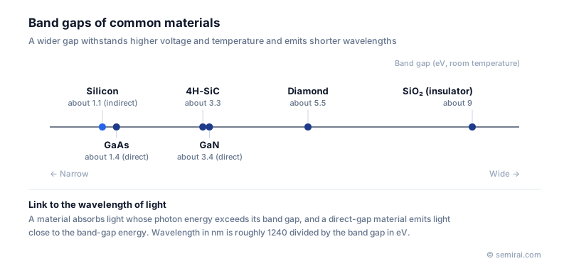
Room-temperature values are about 0.66 eV for germanium, 1.12 eV for silicon, 1.42 eV for GaAs, 3.26 eV for 4H-SiC and 3.4 eV for GaN. A wider gap means a much higher critical electric field before breakdown, so a thinner, more heavily doped drift layer can block the same voltage, and the intrinsic carrier count stays low at high temperature. That is why SiC and GaN are used in EV inverters, chargers and power supplies.
The gap also sets the optical behaviour. A material absorbs photons with more energy than its gap, and the wavelength in nanometres is roughly 1240 divided by the gap in eV. Silicon therefore absorbs visible and near-infrared light up to about 1.1 µm, while InGaN alloys emit blue and green light.
Direct and indirect band gaps
In a direct-gap material (GaAs, InP, GaN) the conduction-band minimum and valence-band maximum occur at the same crystal momentum, so an electron and hole can recombine by emitting a photon. In an indirect-gap material (silicon, germanium, SiC) the recombination also needs a lattice vibration (phonon), so light emission is very weak. LEDs and lasers use direct-gap compounds; silicon is used for integrated circuits, solar cells and image sensors, where it only has to absorb light.
Japanese companies involved
- Nichia makes GaN-based blue and white LEDs and laser diodes, whose light comes from the wide, direct band gap of InGaN.
- ROHM, Mitsubishi Electric and Fuji Electric make SiC power devices that rely on SiC's wide band gap for high-voltage switching.
- Nichia · LEDs and laser diodes
- ROHM · SiC and silicon power devices, analog ICs
- Mitsubishi Electric (power devices) · IGBT and SiC power modules, RF and optical devices
- Fuji Electric (power semiconductors) · IGBT modules and SiC power devices
FAQ
Why does a wider band gap give a higher breakdown voltage?
Breakdown starts when carriers gain enough energy from the field to knock new electron-hole pairs free. A wider gap needs more energy for this, so the critical field rises steeply: for 4H-SiC and GaN it is roughly ten times that of silicon.
How is the band gap measured?
Usually optically. The absorption edge, where the material starts to absorb light, and photoluminescence, the light emitted when excited carriers recombine, both reveal the gap. The temperature dependence of intrinsic conductivity gives an electrical estimate.
Can the band gap be tuned?
Yes, by alloying. Changing the indium content of InGaN moves LED emission from violet towards green, and AlGaAs or SiGe alloys shift the gap of GaAs or silicon. Strain and quantum-well confinement also shift the effective gap.
Related pages
Sources
Last updated: November 2, 2026