IGZO (Indium Gallium Zinc Oxide)
IGZO is an oxide semiconductor made of indium (In), gallium (Ga), zinc (Zn) and oxygen (O). Electrons move well in it even when the atoms are arranged irregularly in an amorphous film. It is used in the thin-film transistors that drive display pixels and is being studied for memory and logic.
Also called: a-IGZO, InGaZnO, oxide semiconductor
Diagram
Why IGZO suits displays
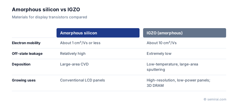
In 2004 Hideo Hosono's group at Tokyo Institute of Technology (now Institute of Science Tokyo) reported thin-film transistors (TFTs) made from amorphous IGZO. Its electron mobility is around 10 cm²/Vs, more than ten times that of the amorphous silicon long used in LCD panels. It can be deposited uniformly on large glass substrates by sputtering at low temperature, which suits large panels.
The other key property is very low off-state leakage current. When an image does not change, the pixel transistors can be switched off and the stored voltage holds, so the panel can refresh less often and use less power.
From displays to memory
Low leakage is also attractive for memory. In a DRAM cell, charge leaks out of the capacitor, mostly through the access transistor, so every cell must be refreshed many times a second. An IGZO access transistor could hold the charge much longer and reduce how often refresh is needed.
Because IGZO can be deposited at low temperatures, it can be built within or above the wiring layers of a chip without damaging what lies below. This makes it a candidate for 3D DRAM and for monolithic 3D integration, and memory makers and research institutes are developing it for those uses.
Japanese companies involved
- IGZO thin-film transistors originated in research at Tokyo Institute of Technology (now Institute of Science Tokyo) and were first commercialised in Japanese LCD panels.
- JX Advanced Metals makes sputtering targets, the category of material used to deposit oxide semiconductor films such as IGZO.
- JX Advanced Metals · Sputtering targets and high-purity metals
FAQ
How does IGZO compare with LTPS?
Low-temperature polysilicon (LTPS) has higher mobility and is used in high-resolution smartphone panels, but it is harder to make uniformly over very large substrates. IGZO has lower mobility, yet it is easier to deposit uniformly on large glass and has much lower off-state leakage, so it suits large and low-power panels. Some panels combine both.
Is IGZO crystalline or amorphous?
Both forms exist. Most display TFTs use amorphous IGZO because it is uniform over large areas. Crystalline variants, such as c-axis aligned crystalline IGZO (CAAC-IGZO), have also been developed to improve stability and are used in some products and memory research.
Related pages
- Leakage Current
- Sputtering
- Sputtering Target
- Semiconductor materials (wafers and substrates)
- Sputtering targets
- JX Advanced Metals Cu and Ta sputtering targets for semiconductors
- Shin-Etsu Chemical 300 mm silicon wafers
- SUMCO Polished wafers (PW)
- Sumitomo Electric Industries (compound semiconductors) GaAs and InP substrates
Sources
Last updated: November 12, 2026