Miller Index
Miller indices are a notation that uses a set of three integers to identify planes and directions in a crystal. Planes are written in round brackets, such as (100), (110) and (111), and directions in square brackets, such as [100]. In semiconductor manufacturing they are the standard way to specify the surface orientation of a wafer.
Also called: Miller indices, (hkl)
Diagram
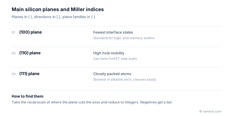
How Miller indices are found
To find the indices of a plane, take the points where it crosses the three crystal axes, expressed in units of the lattice constant. Take the reciprocals of these intercepts and multiply them by the smallest number that turns them into integers. A plane parallel to an axis has an infinite intercept, whose reciprocal is zero. For example, a plane crossing the x axis at 1 and parallel to y and z is (100). A negative intercept is shown with a bar over the number.
Brackets carry meaning. Round brackets (hkl) denote one plane, curly brackets {hkl} denote the family of equivalent planes, square brackets [uvw] denote a direction and angle brackets denote the family of equivalent directions. In a cubic crystal such as silicon, the direction [hkl] is perpendicular to the plane (hkl).
Why the plane matters in chipmaking
Different planes have different atom densities and bond arrangements, so oxidation rate, etch rate, carrier mobility and interface quality all depend on orientation. CMOS logic and memory are built mainly on (100) wafers because the silicon/oxide interface on that plane has the lowest density of interface states.
The (110) plane gives higher hole mobility and can appear as the side wall of FinFET fins. The {111} planes etch extremely slowly in alkaline solutions such as KOH, so anisotropic wet etching of a (100) wafer leaves V-grooves and pyramid-shaped pits bounded by {111} planes, a basic tool of MEMS fabrication. Silicon also cleaves most easily along {111} planes.
FAQ
Why is (200) not simply written as (100)?
In crystallography (200) describes a set of planes with half the spacing of (100), which matters in X-ray diffraction. When only the orientation is meant, as with wafer surfaces, the indices are reduced to the smallest integers, so the surface is called (100).
How are Miller indices written for hexagonal crystals?
Hexagonal crystals such as GaN and SiC usually use four-index Miller-Bravais notation (hkil), where i = -(h + k). For example, the c-plane is (0001), the m-plane is (1-100) with a bar over the 1, and the a-plane is (11-20). This keeps equivalent planes looking alike.
Related pages
Sources
Last updated: November 2, 2026