Lattice Constant
The lattice constant is the edge length of the unit cell, the repeating unit in which atoms are regularly arranged in a crystal. Silicon has a lattice constant of about 0.543 nm. When a film and its substrate have different lattice constants, the mismatch creates strain and, beyond a critical thickness, misfit dislocations, so it governs which materials can be grown on each other.
Also called: lattice parameter
Diagram
Typical values
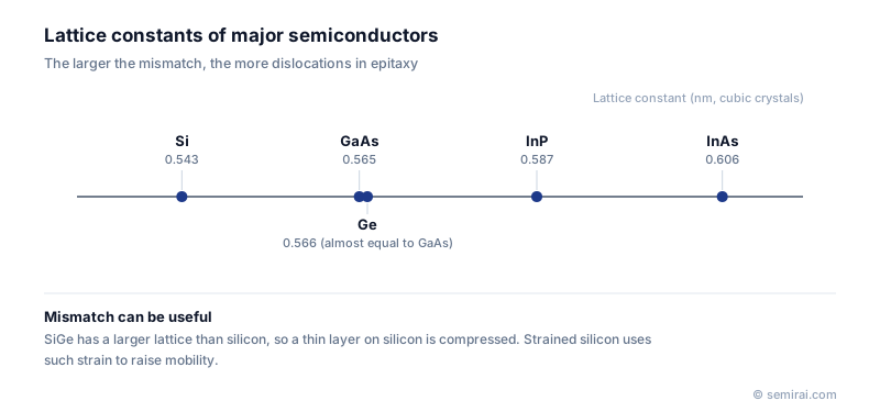
Each crystal has characteristic values. Cubic crystals are described by one number, a, while hexagonal crystals such as GaN and SiC need two, the base edge a and the height c. At room temperature, silicon (diamond structure) is about 0.543 nm, germanium about 0.566 nm, GaAs about 0.565 nm, InP about 0.587 nm and InAs about 0.606 nm. Hexagonal GaN has a ≈ 0.319 nm, and 4H-SiC has a ≈ 0.308 nm.
GaAs and AlAs have almost the same lattice constant, so their alloy AlGaAs can be grown on GaAs without strain. This made AlGaAs/GaAs the classic heterojunction. On InP substrates, the compositions of InGaAs and InGaAsP are adjusted so that their lattice constants match InP, which is how optical-communication lasers and photodiodes are made. Lattice constants are measured precisely by X-ray diffraction.
Lattice mismatch and strain
Lattice mismatch is expressed as the difference between the film's and the substrate's lattice constants divided by the substrate's. When the mismatch is small and the film is thin, the film stretches or compresses elastically to fit the substrate. Above a critical thickness, the stored strain is relieved by misfit dislocations at the interface, and threading dislocations that run up through the film raise leakage and reduce light emission.
GaN on silicon has a mismatch of roughly 17 percent, so GaN-on-Si wafers rely on buffer layers to manage dislocations and wafer bow. Mismatch can also be useful. In strained-silicon technology, SiGe, which has a larger lattice than silicon, is grown in the source and drain of p-type transistors, squeezing the silicon channel and raising hole mobility.
FAQ
What does lattice-matched mean?
It means the film and the substrate have the same, or nearly the same, lattice constant. A lattice-matched layer grows without significant strain, so even thick layers stay free of misfit dislocations. Compound alloys are usually tuned in composition to achieve this.
Does the lattice constant change with temperature?
Yes, it increases slightly as the crystal expands. If the film and substrate expand at different rates, a structure that is matched at growth temperature becomes strained on cooling, which can bow or crack the wafer. Thermal expansion mismatch is a major issue for GaN on silicon.
Related pages
- Crystal Structure
- Epitaxy (Epitaxial Growth)
- Heterojunction
- Dislocation
- GaN-on-Silicon (GaN-on-Si)
- Miller Index
- Gallium Arsenide (GaAs)
- Indium Phosphide (InP)
- Epitaxial growth equipment
- Compound semiconductor wafers
- Kokusai Electric QUIXACE®-LV
- NuFlare Technology EPIREVO™ S6
- NuFlare Technology EPIREVO™ S8
- Resonac InP epitaxial wafers
Sources
Last updated: November 13, 2026