MEMS (Micro-Electro-Mechanical Systems)
MEMS (micro-electro-mechanical systems) are devices that use semiconductor microfabrication to build mechanical structures, such as moving masses, membranes, mirrors and fluid channels, together with electrical circuits. Their moving parts range from micrometres to millimetres in size and convert physical quantities into electrical signals, or electrical signals into motion.
Also called: micromachines, microsystems
Diagram
Where MEMS are used
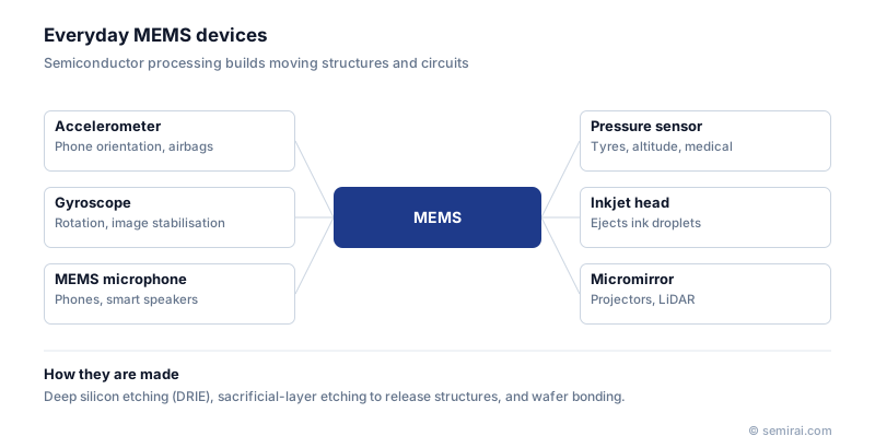
Most people carry several MEMS devices in their phone. Accelerometers and gyroscopes detect orientation and movement and support image stabilisation. MEMS microphones pick up voice in phones and smart speakers, and pressure sensors measure air pressure for altitude or tyre pressure in cars. Cars also use MEMS accelerometers for airbag triggering.
Other examples are inkjet print heads, which eject ink droplets through microscopic nozzles, and micromirror arrays such as the digital micromirror device in projectors. Scanning micromirrors are also used in some LiDAR systems. Biomedical chips that move small volumes of liquid through micro-channels are another growing class.
Processes specific to MEMS
MEMS fabrication starts from ordinary semiconductor steps such as lithography, CVD and sputtering, then adds techniques for building three-dimensional structures. Deep reactive ion etching (DRIE) cuts vertical trenches tens to hundreds of micrometres deep into silicon by alternating etch and passivation steps. Sacrificial-layer etching removes a layer underneath a structure so that it is released and free to move. Wafer bonding, such as anodic, direct or low-temperature bonding, seals cavities and caps the moving parts.
Some MEMS are integrated with CMOS circuits on the same chip, while others are made on a separate die and packaged with an ASIC. Wafer-level packaging is widely used to protect the fragile structures and to reduce size and cost.
Japanese companies involved
- Sumitomo Precision Products makes deep silicon etching equipment used to form MEMS structures.
- Murata Manufacturing makes MEMS sensors, and Seiko Epson uses MEMS technology in its inkjet print heads.
- Murata Manufacturing · Capacitors, RF modules, SAW/BAW filters and MEMS sensors
- Tokyo Electron (TEL) · Coat/develop, etch and deposition equipment
- Sumitomo Precision Products · MEMS and semiconductor manufacturing equipment (deep silicon etching)
FAQ
Are MEMS made in ordinary semiconductor fabs?
Partly. MEMS can use older lithography generations, so many are made on 150 mm or 200 mm lines, but they need special tools for deep etching, release and bonding. Large MEMS makers run dedicated fabs, and fabless designers use MEMS foundries.
Why is packaging a MEMS device difficult?
The moving structure must be protected from dust, moisture and stress, yet some devices, such as microphones and pressure sensors, need an opening to the outside world. Package stress can also shift the sensor output, so the package is designed together with the device.
Related pages
Sources
Last updated: November 13, 2026