Sputtering
Sputtering is a physical vapour deposition (PVD) method in which an inert gas such as argon is turned into a plasma inside a vacuum chamber and its ions are driven into a target. Atoms knocked out of the target travel to the wafer and build up a thin film of metal or compound.
Also called: sputter deposition, PVD
Diagram
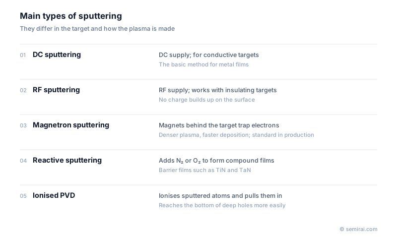
Types of sputtering
DC sputtering uses a direct-current supply and works for conductive targets. RF sputtering uses a radio-frequency supply so that charge does not build up on insulating targets. Magnetron sputtering places magnets behind the target to trap electrons near its surface, which makes the plasma denser and deposition faster; it is the standard method in volume production.
Adding nitrogen or oxygen to the argon gives reactive sputtering, which forms compound films such as titanium nitride (TiN) and tantalum nitride (TaN). In ionised PVD, many sputtered atoms are ionised and pulled towards the wafer by a bias voltage, so they land closer to vertical and reach the bottom of deep holes.
Where sputtering is used
Sputtering deposits interconnect metals such as aluminium and copper seed layers, barrier metals such as Ti, TiN, Ta and TaN, and adhesion layers for tungsten contacts. In copper damascene wiring, a TaN/Ta barrier and a copper seed layer are sputtered into each trench before the trench is filled by electroplating.
Compared with chemical vapour deposition, sputtering runs at low temperature, from room temperature to a few hundred degrees, and gives pure, well-adhering films. Its weakness is step coverage: atoms arrive mostly in straight lines, so the sidewalls and bottoms of high-aspect-ratio holes receive less material. For the narrowest features some layers have moved to atomic layer deposition.
Japanese companies involved
- ULVAC makes sputtering systems and other vacuum deposition equipment for semiconductors and electronic components.
- Canon ANELVA builds sputtering and vacuum deposition equipment, including systems for magnetic and metal films.
- ULVAC · Vacuum deposition (sputtering) equipment and vacuum pumps
- Canon ANELVA · Sputtering and vacuum deposition equipment
FAQ
Why is argon used for sputtering?
Argon is chemically inert, so it does not react with the film, and its atoms are heavy enough to transfer momentum efficiently to the target atoms. It is also abundant and inexpensive, which matters because a steady flow is used in every process run.
What is the difference between sputtering and evaporation?
Both are PVD methods. Evaporation heats the source until atoms boil off, and those atoms travel in very straight lines. Sputtering ejects atoms by ion impact, which works for metals with very high melting points and keeps alloy compositions close to the target's.
What limits sputtering at advanced nodes?
As vias become narrower and deeper, straight-line deposition leaves overhangs at the opening and thin films at the bottom. Ionised PVD and other directional techniques push the method further, but the thinnest conformal barriers are increasingly made by ALD.
Comparisons
Related pages
Sources
Last updated: November 13, 2026