Indium Phosphide (InP)
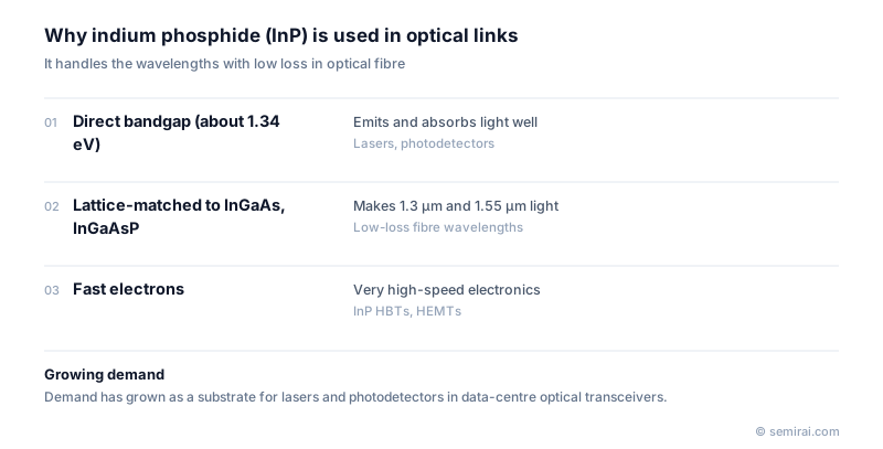
Indium phosphide (InP) is a III-V compound semiconductor made of indium and phosphorus, with a direct bandgap of about 1.34 eV. Alloys such as InGaAs and InGaAsP can be grown on it with matching lattice constants, and these can emit and detect light at 1.3 µm and 1.55 µm, the wavelengths where optical fibre has the lowest loss.
Also called: InP
Diagram
Optical communication devices
Optical fibre transmits light with the least loss and dispersion around 1.3 µm and 1.55 µm. Silicon cannot emit light efficiently, and GaAs-based materials do not reach these wavelengths easily, so InP is the standard platform. Lasers for long-distance links and data-centre transceivers, such as DFB (distributed feedback) lasers and EMLs (electro-absorption modulated lasers), are built on InP. So are InGaAs photodiodes and avalanche photodiodes and many optical modulators.
Silicon photonics, which forms waveguides and modulators in silicon, still needs a light source, and InP-based lasers are attached or bonded to supply it. The growth of high-speed optical links inside data centres has made InP devices and substrates more important.
Electronic uses and supply
Electrons move fast in InP and in InGaAs grown on it, so InP HBTs and HEMTs operate well above 100 GHz and are used in test instruments and research on future wireless systems. InGaAs on InP is also used in short-wave infrared (SWIR) image sensors.
InP crystals are grown by the VGF or LEC method. They are brittle and hard to grow with few defects, so wafers are mostly 2 to 4 inches in diameter, with 6-inch wafers starting to appear. The substrates cost more than GaAs or silicon and come from a small number of suppliers. Indium itself is a minor metal recovered mainly as a by-product of zinc refining.
Japanese companies involved
- JX Advanced Metals and Sumitomo Electric Industries make InP substrates used for optical-communication devices.
- JX Advanced Metals · Sputtering targets and high-purity metals
- Sumitomo Electric Industries (compound semiconductors) · SiC epitaxial wafers and GaAs and InP substrates
FAQ
Why is InP wafer processing difficult?
InP is softer and more brittle than silicon and cleaves easily, so thinning and dicing can cause chipping and cracks. Grinding, polishing and handling are adapted to the material, and lasers are often separated by cleaving to form their mirror facets.
How does an InP laser differ from a VCSEL?
Most InP communication lasers are edge-emitting: light leaves from a cleaved facet at the side of the chip. VCSELs emit from the top surface and are mainly made on GaAs for shorter wavelengths around 850 nm, used over short multimode fibre links.
Related pages
- Compound Semiconductor
- Gallium Arsenide (GaAs)
- Phosphorus (P)
- Heterojunction
- Lattice Constant
- Substrate
- Vertical Bridgman Method (VB)
- MBE (Molecular Beam Epitaxy)
- Compound semiconductor wafers
- Compound semiconductor equipment
- MOCVD equipment
- Sumitomo Electric Industries (compound semiconductors) GaN substrates
- Canon ANELVA EC8100
- EpiQuest MPC6100
- EpiQuest SH series
Sources
Last updated: November 13, 2026