Sputtering Target
A sputtering target is a plate of metal or compound that supplies the film material in sputtering. Argon ions from a plasma strike it and knock out atoms, which deposit on the wafer. Semiconductor targets include aluminium, copper, titanium, tantalum, cobalt and tungsten, and some of their compounds.
Also called: sputter target, PVD target
Diagram
What a semiconductor target must meet
Purity is typically 5N (99.999%) to 6N (99.9999%). Alkali metals such as sodium shift transistor characteristics, and radioactive elements such as uranium and thorium emit alpha particles that can flip memory bits, so even traces must be removed.
The metallurgy also matters. Controlling grain size and crystal orientation makes the film thickness more uniform and reduces particles, and the target must be free of internal voids and inclusions that could cause arcing. Producing large targets that meet all these requirements is a specialised field of materials processing.
Structure and use
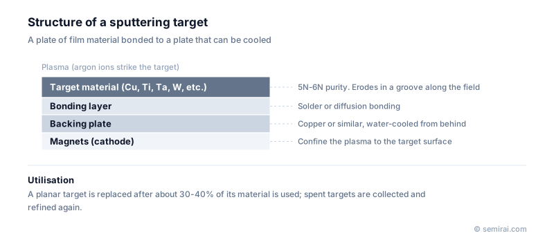
The target is bonded to a backing plate, often copper, by soldering or diffusion bonding, and the assembly is water-cooled from behind during sputtering. In a magnetron system the magnetic field concentrates the plasma, so the target erodes in a groove called the erosion track.
With a planar target only about 30-40% of the material is consumed before the groove gets too deep and the target must be replaced. Used targets are collected and the remaining metal is refined and reused. Rotating magnets and target shape design are used to spread erosion more evenly and raise utilisation.
Japanese companies involved
- JX Advanced Metals makes high-purity sputtering targets for semiconductor interconnects and barrier layers.
- Tosoh and Mitsubishi Materials also produce sputtering targets, and Furuya Metal specialises in targets made from platinum-group metals.
- Tosoh · Sputtering targets, ALD/CVD precursors and quartz glass
- Mitsubishi Materials · High-purity polysilicon and electronic materials
- JX Advanced Metals · Sputtering targets and high-purity metals
- Furuya Metal · Platinum-group metal sputtering targets and catalysts
FAQ
Why does a target need such high purity?
Impurities in the target end up in the film. Sodium and potassium are mobile in oxides and move threshold voltages, transition metals can create leakage, and alpha-emitting uranium and thorium cause soft errors in memory. Purity of 5N to 6N keeps these effects acceptably small.
Why can't the whole target be used?
The magnetron plasma is densest where the magnetic field lines run parallel to the surface, so only that region erodes quickly. The target has to be replaced before the groove breaks through to the backing plate, leaving most of the material unused but recyclable.
Related pages
- Sputtering
- Magnetron Sputtering
- Barrier Metal (Diffusion Barrier)
- Copper (Cu)
- Tungsten (W)
- IGZO (Indium Gallium Zinc Oxide)
- Sputtering targets
- Sputtering equipment
- JX Advanced Metals Cu and Ta sputtering targets for semiconductors
- Tosoh Metal targets (Mo, Cu, Ti and others)
- Canon ANELVA FC7100
- Canon ANELVA IC7500
Sources
Last updated: November 13, 2026