MPW (Multi-Project Wafer)
An MPW (multi-project wafer) is a prototyping service in which chips from several customers or designs share one mask set and are made together on the same wafers. Participants split the cost of masks and fabrication, so prototyping is far cheaper than ordering a dedicated mask set. Because runs depart on a fixed schedule, MPW services are also called shuttles.
Also called: shuttle, multi-project wafer run
Diagram
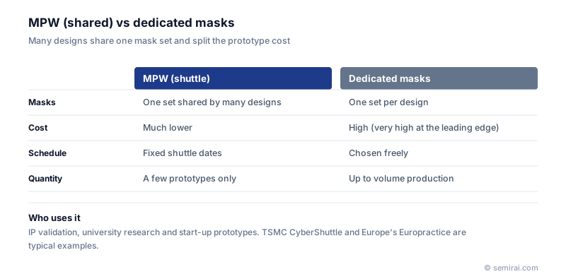
Who uses MPW and how
A foundry or a broker organisation announces run dates and collects designs. Each participant buys an area on the reticle, the designs are tiled together, and after fabrication each participant receives a small batch of its own dies. Typical users are companies validating a new design before volume production, IP vendors proving that their blocks work in silicon, universities and research institutes, and start-ups building first prototypes.
Well-known services include TSMC's CyberShuttle, Europractice for European universities and research institutes, and MOSIS in the United States. Because a dedicated mask set at an advanced node is very expensive, MPW is often the only realistic way for small companies and researchers to try a leading-edge process.
Limits of MPW
Die area is limited to the slot purchased, often a few millimetres on a side, and only tens to hundreds of chips are delivered, so MPW chips are not suitable for production. The foundry sets the schedule, so the design must be ready by the tape-out deadline. Once a prototype works, the usual next step is a dedicated mask set for volume production.
Open process design kits and open-source EDA tools have widened access. Programmes based on the open SkyWater 130nm process, for example, have offered free or low-cost shuttles that let students and individuals design and fabricate real chips.
Japanese companies involved
- In Japan, the University of Tokyo's VDEC programme has long given universities access to chip fabrication runs for design education and research, a role similar to that of MPW brokers abroad.
- Rapidus · Leading-edge logic foundry (2 nm, in development)
FAQ
Why is MPW cheaper?
Masks and wafer processing are a large share of prototyping cost, and in an MPW run they are shared among all participants in proportion to the area each uses. At advanced nodes, where a full mask set is extremely expensive, the saving is large.
Can chips from an MPW run go straight into a product?
Generally not. Quantities are small, die size is constrained and timing depends on the shuttle schedule. After verifying the design on MPW chips, companies order a dedicated mask set for production.
Comparisons
Related pages
Sources
Last updated: November 2, 2026