Photomask / Reticle
A photomask is the master plate used in lithography to transfer one layer of an integrated circuit onto the resist on a wafer. The pattern is formed in a chrome or molybdenum-silicide film on a transparent quartz substrate, and its accuracy carries straight into the chip. Masks for EUV lithography are reflective rather than transparent.
Also called: mask, reticle
Diagram
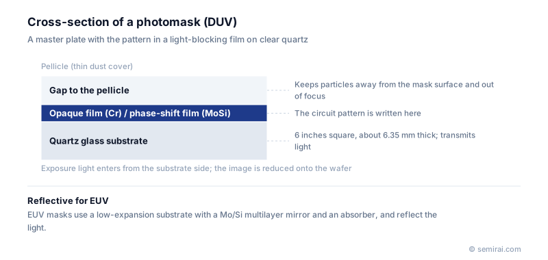
Structure and how masks are made
A standard mask blank is a quartz plate 6 inches square and about 6.35 mm thick, coated with an opaque chrome film or a phase-shift film of molybdenum silicide (MoSi), and then with resist. An electron-beam mask writer draws the pattern, which is developed and etched into the film. The mask is then inspected, defects are repaired, and it is cleaned.
Projection tools reduce the image by four times, so the mask pattern is four times larger than on the wafer. A thin transparent membrane called a pellicle is mounted a few millimetres above the pattern so that any particle that lands on it is out of focus and does not print.
Why masks have become complex
As features shrank below the wavelength, the printed shape stopped matching the drawn shape. Optical proximity correction (OPC) adds serifs, biases and sub-resolution assist features so the wafer image comes out right, and phase-shift masks use film thickness to shift the phase of the light and sharpen edges. These corrections greatly increase the amount of data and writing time per mask.
EUV masks reflect light instead. They use a low-thermal-expansion substrate coated with a molybdenum-silicon multilayer mirror and a patterned absorber. A defect buried in the multilayer can print, so EUV mask blanks need especially strict inspection, and pellicles must be thin enough to transmit EUV light while surviving its heat.
Japanese companies involved
- Dai Nippon Printing (DNP) and TOPPAN are major merchant photomask makers serving chipmakers worldwide.
- HOYA, AGC and Shin-Etsu Chemical supply mask blanks, with HOYA and AGC both producing EUV mask blanks.
- NuFlare Technology makes electron-beam mask writers, and Lasertec makes mask and mask blank inspection systems.
- TOPPAN Holdings · Photomasks and FC-BGA package substrates
- HOYA · Mask blanks (including EUV) and photomasks
- AGC · EUV mask blanks and glass materials
- NuFlare Technology · Electron-beam mask writers, mask inspection and epitaxial reactors
- Lasertec · EUV mask and mask blank inspection
- Shin-Etsu Chemical · Silicon wafers, photoresists and photomask blanks
- Dai Nippon Printing (DNP) · Photomasks and lead frames
FAQ
What is the difference between a photomask and a reticle?
Strictly, a photomask carried the whole wafer pattern at 1:1, while a reticle carries one exposure field at a larger scale for reduction projection. Since practically all front-end lithography now uses reduction projection, the two words are used interchangeably.
How many masks does a chip need?
Each patterned layer needs its own mask, and multi-patterned layers need several. A mature-node chip may use a few dozen masks, while leading-edge logic uses many more, which is why a full mask set for an advanced chip is a major cost.
Who makes photomasks?
Leading foundries and memory makers run their own mask shops for their most advanced layers. Merchant mask makers such as DNP, TOPPAN and Photronics supply the rest of the market.
Related pages
- Lithography Equipment
- EUV Lithography Equipment (EUV Scanner)
- Reticle / Photomask
- EUV (Extreme Ultraviolet)
- Actinic inspection
- Registration
- Inverse Lithography Technology (ILT)
- NRE (Non-Recurring Engineering) Cost
- Electron-beam mask writers
- NuFlare Technology EBM-8000P/H / EBM-8000P/M
- NuFlare Technology EBM-9500PLUS
- NuFlare Technology MBM™-2000
- NuFlare Technology MBM™-2000PLUS
Sources
Last updated: November 13, 2026