Photonics-Electronics Convergence
Photonics-electronics convergence is the umbrella term for technologies that integrate electronic chips, which process signals electrically, as closely as possible with optical circuits that transmit them as light, progressively replacing electrical data transmission with optical links. It is driven by AI and data centres, where the speed and power of electrical wiring between chips and servers are reaching their limits.
Also called: optoelectronic integration, opto-electronic convergence
Diagram
Why move from electrical to optical
Electrical links lose more signal as distance and data rate increase, so they need more power in the SerDes and equalisation circuits that clean up the signal. Optical fibre and waveguides have very low loss over distance, and many wavelengths can share one fibre (wavelength division multiplexing), carrying far more data per link. For AI clusters, where huge amounts of data move between accelerators, optical links can cut both energy per bit and latency.
Bringing optics step by step closer to the chip
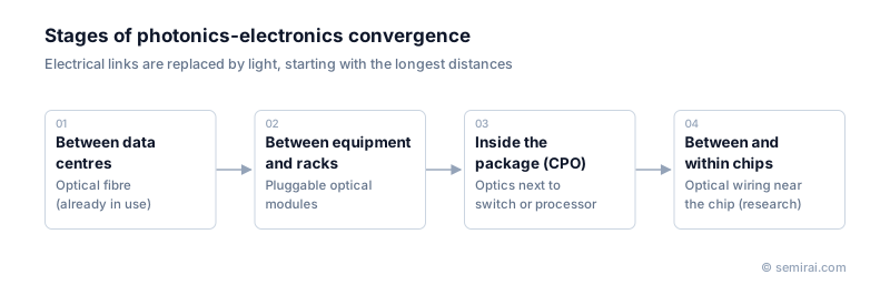
Optics has moved inward in stages. Links between data centres have long been optical. Links between racks and equipment use pluggable optical transceiver modules. The next stage is co-packaged optics (CPO), in which optical engines sit in the same package as a switch or processor chip. The final stage, still in research, is optical wiring between chips and even within them.
Several technologies are needed: silicon photonics, which builds waveguides, modulators and detectors on silicon wafers; integration of lasers made from compound semiconductors such as indium phosphide with silicon; advanced packaging that connects optical and electronic chips densely; and thermal management, because optical devices are sensitive to temperature.
Japanese companies involved
- NTT places photonics-electronics convergence at the core of its IOWN (Innovative Optical and Wireless Network) concept and is developing devices for it, supported by national research programmes.
- Sumitomo Electric Industries makes indium phosphide substrates and optical devices used in optical communication.
- Sumitomo Electric Industries (compound semiconductors) · SiC epitaxial wafers and GaAs and InP substrates
FAQ
How is it different from silicon photonics?
Silicon photonics is a specific technology for building optical circuits on silicon wafers. Photonics-electronics convergence is the broader goal of combining optical and electronic circuits and moving transmission to light, using silicon photonics among other technologies.
What does it improve?
Mainly the energy and delay of moving data, and the amount of data that can be moved. Electrical links need more power to compensate for losses as speeds rise, while light keeps losses low over distance, which matters most in AI data centres.
Related pages
Sources
Last updated: November 2, 2026