Multilevel Interconnect
Multilevel interconnect is the structure of many metal wiring layers, separated by insulating films, that connects the billions of transistors on a silicon chip. Leading-edge logic chips have more than ten layers, joined vertically by vias. The part of the manufacturing flow that builds this wiring is called the back end of line (BEOL).
Also called: BEOL, metal stack, multilayer wiring
Diagram
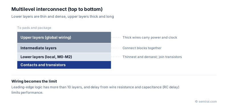
How the layers are organised
Wiring is arranged in a hierarchy. The lowest layers, often called M0 to M2, are local interconnect directly above the transistors; they are the thinnest and densest and connect transistors within a cell. Intermediate layers link cells and blocks. The top global layers are thick and widely spaced, carrying power, ground and clock signals across the chip and up to the package bumps. Each layer is separated by an interlayer dielectric (ILD), and the design of vias and dielectrics strongly affects delay and power.
Why interconnect limits performance
As wires become narrower, their resistance (R) rises, and as they move closer, the capacitance (C) between them rises. The product sets RC delay, and at advanced nodes wiring delay, not transistor speed, often decides how fast a chip can run. To manage this, the industry moved from aluminium to copper wiring formed by the damascene method in the late 1990s, and replaced silicon dioxide between lines with low-k dielectrics.
At the newest nodes further measures are being added: air gaps to cut capacitance, cobalt and ruthenium for the narrowest lines where copper's resistance rises sharply, and backside power delivery, which moves the power network off the front-side stack altogether. Chemical mechanical planarization (CMP) after each layer keeps the surface flat enough for the next one to be patterned.
Japanese companies involved
- Tokyo Electron supplies deposition, etch and coater/developer equipment used to build interconnect layers.
- Ebara makes CMP systems, and Resonac and Fujimi supply CMP slurries used to planarise copper and dielectric layers.
- Ebara · CMP systems, dry vacuum pumps and exhaust treatment
- Resonac · CMP slurries, packaging materials and SiC epitaxial wafers
- Fujimi Incorporated · CMP slurries and polishing materials
- Tokyo Electron (TEL) · Coat/develop, etch and deposition equipment
FAQ
How many wiring layers does a chip have?
Leading-edge logic chips commonly have more than ten and up to around fifteen or more metal layers. Simpler or mature-node chips may have only a few. Memory chips need fewer wiring layers than logic because their circuits are highly repetitive.
What is a via?
A via is a small vertical metal plug that connects a wire in one layer to a wire in the layer above or below. Via resistance has become a significant part of total wiring resistance at advanced nodes.
How is RC delay reduced?
Lower-resistance metals reduce R, and lower-k insulators or air gaps reduce C. Designers also insert repeaters on long wires and route critical signals on thicker upper layers.
Related pages
Sources
Last updated: November 1, 2026