Reticle / Photomask
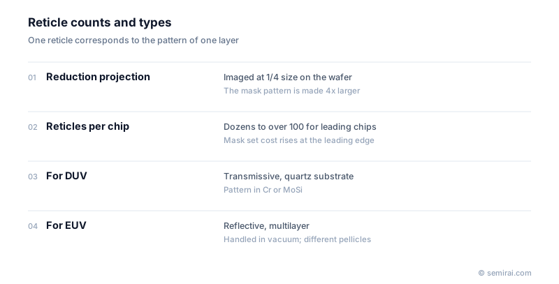
A reticle is the photomask used in reduction projection lithography: a quartz plate carrying one layer's pattern, usually at four times the size it will have on the wafer. The exposure tool projects it onto one field at a time. Because each patterned layer needs its own reticle, an advanced chip needs a set of dozens or more.
Also called: reticle, photomask, mask
Diagram
From design data to reticle
Before writing, the layout is processed by optical proximity correction (OPC) software. Diffraction and interference make the printed image differ from the drawn shape, rounding corners and shortening line ends, so OPC deliberately distorts the reticle pattern to compensate. For leading-edge layers this is a large computing job, and inverse lithography techniques that compute curvilinear mask shapes are increasingly used.
An electron-beam writer then draws the corrected pattern into resist on a mask blank, followed by development, etching of the chrome or phase-shift film, inspection, repair and cleaning. Multi-beam writers have made curvilinear patterns practical to write.
Protecting and handling reticles
A pellicle, a thin membrane stretched over a frame, keeps particles off the patterned surface. For DUV, pellicles are mature polymer films. EUV pellicles must transmit 13.5 nm light twice, in and out, while surviving high temperatures inside the scanner, so they are made from very thin inorganic films and remain a demanding component.
EUV reticles are reflective, with a molybdenum-silicon multilayer and a patterned absorber, and are carried in special dual pods that protect them from particles. Reticles are inspected regularly during use, since a single repeating defect would print on every field of every wafer.
Japanese companies involved
- NuFlare Technology makes electron-beam mask writers, and JEOL also makes electron-beam writing systems.
- Lasertec makes reticle and mask blank inspection systems, including actinic inspection for EUV.
- Shin-Etsu Chemical supplies photomask blanks, and Mitsui Chemicals makes pellicles, including EUV pellicles.
- JEOL · Electron beam lithography systems, electron microscopes and surface analysis
- Mitsui Chemicals · EUV pellicles and wafer protection tapes
- Lasertec · EUV mask and mask blank inspection
- NuFlare Technology · Electron-beam mask writers, mask inspection and epitaxial reactors
- Shin-Etsu Chemical · Silicon wafers, photoresists and photomask blanks
- Elionix · Electron-beam lithography systems
FAQ
What is the difference between a reticle and a photomask?
Strictly, a photomask carries the full wafer pattern at 1:1, and a reticle carries one exposure field at a magnified scale for reduction projection. Because almost all front-end lithography now uses reduction projection, the two words are used as synonyms in practice.
Why is the reticle four times larger than the wafer pattern?
Writing the pattern four times larger relaxes the accuracy needed on the reticle and makes small reticle defects less likely to print. A 4x reduction with a 6-inch reticle also gives a standard 26 × 33 mm exposure field on the wafer.
How are EUV reticles different?
They reflect light rather than transmit it. The blank is a low-thermal-expansion substrate with a multilayer mirror of about 40 molybdenum-silicon pairs, topped by a patterned absorber. Defects buried in the multilayer, pellicle transmission and particle control in vacuum are specific EUV challenges.
Comparisons
Related pages
- Photomask / Reticle
- EUV (Extreme Ultraviolet)
- EUV Lithography Equipment (EUV Scanner)
- Multi-Patterning
- Actinic inspection
- Immersion Lithography (ArFi)
- SMIF Pod
- MPW (Multi-Project Wafer)
- Electron-beam mask writers
- JEOL JBX-3050MV/S
- JEOL JBX-3200MVS
- NuFlare Technology EBM-8000P/H / EBM-8000P/M
- NuFlare Technology EBM-9500PLUS
Sources
Last updated: November 13, 2026