NAND Flash Memory
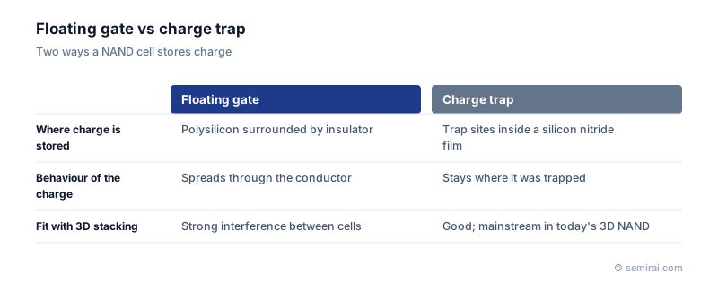
NAND flash is non-volatile memory that stores data as charge held in each cell's floating gate or charge-trap layer, with cells connected in series like a NAND logic gate. The series connection makes each cell very small, so NAND gives the lowest cost per bit of any semiconductor memory and keeps its data without power.
Also called: NAND, 3D NAND
Diagram
How it works
A NAND cell is a transistor with an extra layer that can hold electrons. Adding electrons raises the transistor's threshold voltage, and the controller reads the stored value by checking at which voltage the cell turns on. Cells are written page by page and erased a whole block at a time.
Storing more voltage levels per cell raises capacity: one bit (SLC), two (MLC), three (TLC, the mainstream today) or four (QLC). Each extra bit lowers cost per bit but reduces speed and the number of rewrites the cell can take.
From planar to 3D NAND
Planar NAND stopped shrinking at around 15 nm because neighbouring cells began to disturb each other. The industry turned the array on its side: 3D NAND stacks alternating layers of oxide and nitride (or polysilicon), etches holes through the whole stack and builds the cells around each hole. Samsung started volume production of 3D NAND in 2013, and current products stack more than two hundred layers.
The hardest steps are depositing hundreds of uniform layers, etching channel holes with aspect ratios far above 50:1, and filling them conformally.
Japanese companies involved
- NAND flash was invented at Toshiba, and its memory business is now Kioxia, which makes 3D NAND (BiCS FLASH) at Yokkaichi in Mie and Kitakami in Iwate.
- Tokyo Electron supplies etch and deposition systems used for the high-aspect-ratio steps of 3D NAND.
- Kioxia · NAND flash memory and SSDs
- Tokyo Electron (TEL) · Coat/develop, etch and deposition equipment
FAQ
What is the difference between NAND and NOR flash?
NAND connects cells in series, which makes each cell small and suits high-capacity storage read in pages. NOR connects cells in parallel, so individual bytes can be read quickly at random; it is used to hold boot code and firmware.
Why is NAND built in 3D?
Shrinking the cells in a flat array caused interference between neighbouring cells and left too few electrons per cell. Stacking cells vertically keeps them larger while still raising the number of bits per chip.
What do SLC, MLC, TLC and QLC mean?
They are the number of bits stored per cell: one, two, three and four. More bits per cell means more capacity at lower cost, but lower speed and endurance.
Comparisons
Related pages
Sources
Last updated: November 2, 2026