Dry Etching
Dry etching is the family of etching methods that remove material from a wafer in the gas phase, using a plasma or reactive gases in a vacuum chamber instead of liquid chemicals. Because ions can be driven straight down onto the wafer, it cuts vertical walls, and it is the main way lithography patterns are transferred into films.
Also called: plasma etching, reactive ion etching (RIE)
Diagram
How reactive ion etching works
Most production dry etching is reactive ion etching (RIE). Radio-frequency power turns a process gas into a plasma in a low-pressure chamber. Radicals from the plasma are neutral but chemically active and react with the film to form volatile products that are pumped away. Ions are accelerated by a bias voltage and strike the wafer almost vertically.
The ions supply energy where they land, so the bottom of a feature etches much faster than its sidewalls, and some chemistries also coat the sidewalls with a protective polymer. The pattern goes down without spreading sideways under the mask, which wet etching cannot achieve for features only nanometres wide.
Plasma sources and gas chemistries
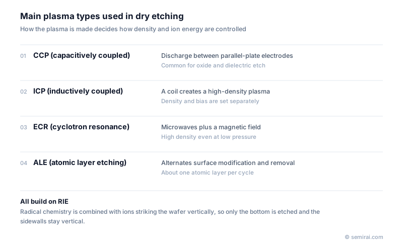
Capacitively coupled plasma (CCP) tools use parallel-plate electrodes and give relatively high ion energy, which suits oxide and other dielectric etching. Inductively coupled plasma (ICP) tools use a coil to create a dense plasma and a separate bias to set ion energy, which suits silicon, gate and metal etching. Electron cyclotron resonance (ECR) sources use microwaves and a magnetic field to keep a dense plasma at low pressure.
Silicon is typically etched with SF₆, Cl₂ or HBr, silicon dioxide with fluorocarbons such as CF₄ or C₄F₈, and silicon nitride with hydrofluorocarbons such as CHF₃. Gas mix, pressure, power and wafer temperature together set the etch rate, the selectivity to the mask and underlying layers, and the profile.
Where dry etching is used
Dry etching shapes transistor gates and fins, opens contact holes and vias, etches back sidewall spacers, cuts shallow trench isolation and drills the deep channel holes of 3D NAND. For the most delicate steps, such as releasing nanosheets in gate-all-around transistors, atomic layer etching (ALE) removes material in self-limiting cycles of roughly one atomic layer each.
Japanese companies involved
- Tokyo Electron (TEL) makes plasma etch systems for dielectric and conductor etching used in high-volume logic and memory fabs.
- Hitachi High-Tech makes dry etch systems based on microwave ECR plasma, and SAMCO makes plasma etching systems used for compound semiconductors, MEMS and research.
- Hitachi High-Tech · CD-SEM metrology, defect inspection and etch systems
- Tokyo Electron (TEL) · Coat/develop, etch and deposition equipment
- SAMCO · Plasma etching, CVD and plasma cleaning equipment
FAQ
What is the difference between dry etching and wet etching?
Wet etching dissolves material in a liquid, usually equally in all directions, so it undercuts the mask. It is still used where it is cheaper or gentler, for example to strip sacrificial layers or etch many wafers at once in a batch.
Is dry etching the same as plasma etching?
In practice the terms overlap, since almost all dry etching uses a plasma. Strictly, dry etching also includes plasma-free gas-phase processes, such as etching silicon with xenon difluoride or removing oxide with anhydrous hydrogen fluoride vapour, which are isotropic and used for release and cleaning steps.
Why is dry etching hard at advanced nodes?
Features are narrower and deeper, so etch rate falls at the bottom of high-aspect-ratio holes, profiles can bow or twist, and dense and sparse areas etch at different speeds. The etch must also stop on layers only a few nanometres thick without damaging them.
Comparisons
Related pages
Sources
Last updated: November 13, 2026