Charge Trap Flash (CTF)
Charge trap flash (CTF) is a type of flash memory cell that stores electrons in defects (traps) inside an insulating silicon nitride layer rather than in a conductive floating gate. Because trapped electrons cannot move, CTF cells interfere less with their neighbours and can be built as continuous films inside vertical holes, which is why most 3D NAND uses them.
Also called: SONOS, TANOS
Diagram
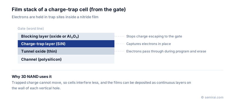
Structure
Seen from the gate, a CTF cell has a blocking layer (silicon oxide or aluminium oxide), a silicon nitride charge-trapping layer, a thin tunnel oxide and the channel. The stack is often called SONOS (silicon-oxide-nitride-oxide-silicon) or TANOS when a tantalum nitride gate and aluminium oxide blocking layer are used.
To program, a high voltage pulls electrons through the tunnel oxide into the nitride, where they are captured. Erasing removes them or injects holes. The amount of trapped charge shifts the cell's threshold voltage, which is how the stored value is read.
Why 3D NAND uses it
In a floating gate cell the charge sits in a conductor, so a single defect in the oxide can drain it, and closely spaced gates couple to each other. In a CTF cell the charge stays where it was trapped. In 3D NAND the oxide, nitride and blocking films are deposited as continuous layers on the inner wall of each channel hole, so a cell is formed wherever a word line crosses the hole.
Making this work requires etching channel holes through hundreds of layers and depositing the cell films uniformly from top to bottom, usually by atomic layer deposition.
Japanese companies involved
- Kioxia's BiCS FLASH 3D NAND uses charge-trap cells.
- Tokyo Electron supplies etch and deposition systems for 3D NAND channel holes and cell films.
- Tokyo Electron (TEL) · Coat/develop, etch and deposition equipment
- Kioxia · NAND flash memory and SSDs
FAQ
What is the difference between charge trap and floating gate?
A floating gate stores charge in a conductive polysilicon layer; a charge trap stores it in an insulating nitride film. Charge in the nitride cannot spread, so CTF cells are more robust to oxide defects and interfere less with their neighbours.
Do all 3D NAND makers use charge trap?
Most do. Samsung, SK hynix, Kioxia and Micron use charge-trap cells in current 3D NAND; Intel's former NAND business, now Solidigm, kept a floating gate design.
Related pages
Sources
Last updated: November 2, 2026