Memory Process
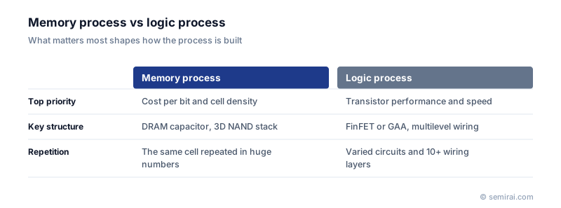
A memory process is a manufacturing technology dedicated to semiconductor memory such as DRAM, NAND flash and NOR flash. Unlike a logic process, which is tuned for transistor speed, a memory process repeats one small cell billions of times, so its main goals are high cell density, low cost per bit and reliable data retention.
Also called: DRAM process, 3D NAND process
Diagram
DRAM: the capacitor problem
A DRAM cell has one transistor and one capacitor (1T1C). As cells shrink, the capacitor must still hold enough charge, so it has grown into a tall cylinder or pillar with a very high aspect ratio. Its dielectric is a high-k stack, typically based on zirconium oxide with aluminium oxide layers, deposited by atomic layer deposition (ALD). Leading DRAM generations are named 1a, 1b (1-beta) and 1c (1-gamma), all in the low-teens nanometre class, and EUV lithography is used on a growing number of layers. Samsung, SK hynix and Micron produce most of the world's DRAM.
3D NAND: building upwards
3D NAND stacks memory cells vertically. Alternating layers of silicon oxide and silicon nitride are deposited by CVD, often more than 200 layers in current products. Channel holes are then etched through the whole stack, which is one of the most demanding etch steps in the industry. A charge-trap silicon nitride layer and a thin polysilicon channel are formed inside the holes, the sacrificial nitride is replaced with tungsten word lines, and a staircase is etched so that each layer can be contacted.
Other memories follow different routes. SRAM, used for on-chip caches, is built in the logic process itself as six-transistor cells. NOR flash is less dense but offers fast random reads, so it remains in use for code storage in microcontrollers and automotive electronics.
Japanese companies involved
- Kioxia develops and manufactures 3D NAND flash at its Yokkaichi and Kitakami plants, jointly with Sandisk.
- Micron Memory Japan produces DRAM in Hiroshima, and Tokyo Electron and Kokusai Electric supply etch and deposition equipment used in memory fabs.
- Kioxia · NAND flash memory and SSDs
- Kokusai Electric · Batch deposition, diffusion and ALD equipment
- Tokyo Electron (TEL) · Coat/develop, etch and deposition equipment
- SCREEN Holdings · Wafer cleaning, coat/develop and inspection equipment
FAQ
Why is high-aspect-ratio etching so important for memory?
Both DRAM capacitors and 3D NAND channel holes are deep, narrow structures. The etch must cut straight through many micrometres of material without bowing or twisting, and every hole on the wafer must look the same, so etch capability often limits how far memory can scale.
Is HBM made with a different process?
The DRAM dies in HBM are made with a DRAM process. What is different is the back-end work: the dies are thinned, given through-silicon vias and stacked, which adds packaging steps to memory production.
Related pages
Sources
Last updated: November 2, 2026