Semiconductor Manufacturing Process
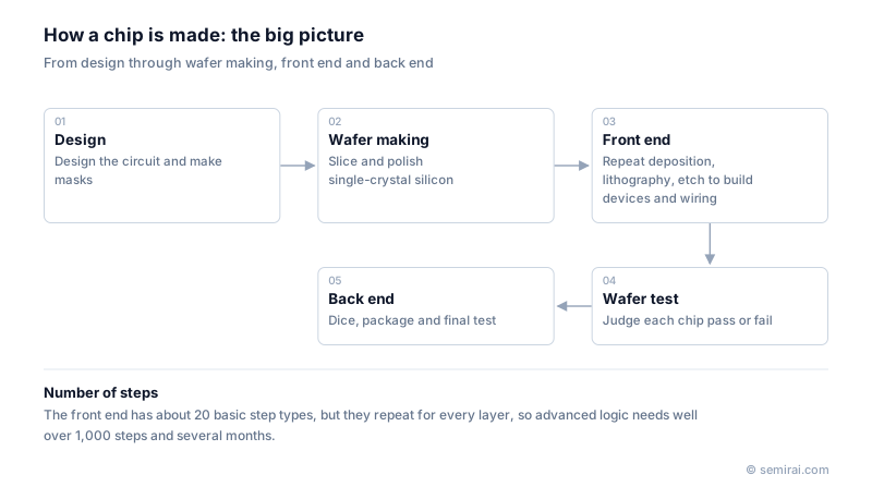
The semiconductor manufacturing process is the full sequence of steps that builds transistors, interconnects and insulating films on a silicon wafer and turns them into working integrated circuits. It is divided into the front end, which forms the devices on the wafer, and the back end, which dices, packages and tests the chips.
Also called: chipmaking process, wafer fabrication process
Diagram
The repeating front-end loop
Front-end processing is built from a small set of unit processes that are repeated many times. The wafer is cleaned, a thin film is deposited by CVD, PVD or ALD, photoresist is coated, exposed with DUV or EUV light and developed, and the pattern is transferred into the film by dry or wet etching. Ion implantation adds dopants where needed, annealing repairs the crystal and activates them, and CMP flattens the surface before the next layer.
Each pass through this loop adds one patterned layer. A modern logic chip needs dozens of such layers for its transistors and interconnects, which is why the total number of steps runs into the hundreds or more.
Process nodes
A technology generation is usually named by its node, such as 7 nm, 5 nm or 3 nm. The name no longer matches any physical dimension on the chip, but each new node packs transistors more densely and improves speed or power efficiency. In return, it needs more lithography steps, tighter control and more expensive tools, so the cost of building and running a leading-edge fab keeps rising.
From finished wafer to product
After the last interconnect layer, every chip on the wafer is probed electrically. The wafer is then thinned and diced, the good dies are mounted and connected in packages, and each packaged part goes through final test before shipment. With 2.5D and 3D packaging and stacked memory such as HBM, the back end has become a source of performance in its own right, not just a protective step.
Japanese companies involved
- Tokyo Electron supplies equipment for many front-end steps, including coat and develop, etch, deposition and cleaning, and SCREEN Holdings is a major maker of wafer cleaning systems.
- Japanese companies also make many of the materials the process consumes, such as silicon wafers, photoresists and high-purity chemicals.
- Tokyo Electron (TEL) · Coat/develop, etch and deposition equipment
- SCREEN Holdings · Wafer cleaning, coat/develop and inspection equipment
FAQ
How long does it take to make a chip?
For an advanced logic or memory chip, front-end processing alone typically takes two to three months from wafer start to finished wafer, because of the large number of steps and the waiting time between tools. Packaging and test add more time.
Why does chipmaking need a cleanroom?
Circuit features are only nanometres to tens of nanometres wide, so a single particle can short or break a line. Cleanrooms filter the air continuously, and workers wear full suits to stop particles shed from the body reaching the wafers.
Where does chip design fit into the process?
Design comes first. The circuit is designed and verified with EDA software, and the layout is converted into a set of photomasks, one for each patterned layer. Manufacturing then follows the masks.
Related pages
Sources
Last updated: November 2, 2026