TSMC N2 Process
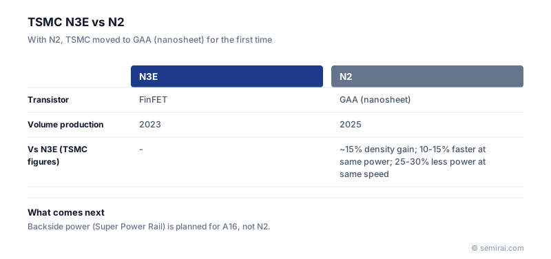
TSMC N2 is TSMC's 2nm-class logic process and the company's first to use gate-all-around (GAA) nanosheet transistors instead of FinFETs. It entered volume production in the fourth quarter of 2025. TSMC states that, compared with N3E, N2 offers 10-15% higher speed at the same power or 25-30% lower power at the same speed, with higher transistor density.
Also called: N2, N2P, TSMC 2nm
Diagram
What is new in N2
The core change is the nanosheet transistor. The channel is a stack of thin silicon sheets surrounded by the gate on every side, which suppresses the short-channel effects that limited further scaling of FinFETs. TSMC also introduced design-technology co-optimisation features such as its NanoFlex standard cells, which let designers mix cells of different heights to balance speed and area.
N2 keeps power delivery on the front of the wafer. Backside power, which TSMC calls Super Power Rail, is not part of N2 or N2P; it is planned for the following A16 process. This differs from Intel, which combined nanosheets and backside power in one step with Intel 18A.
The N2 family
TSMC usually builds a family around each node. After N2 come N2P, a performance-enhanced version, and N2X for higher operating voltages and frequencies, while A16 adds Super Power Rail on top of N2P technology for high-performance computing. Each variant reuses most of the base process, which lets customers move designs with limited rework.
The first N2 products are high-end smartphone and PC processors and AI accelerators. Production is in Taiwan, and EUV lithography is used on many layers.
Japanese companies involved
- TSMC's fabs in Kumamoto are run by JASM, a TSMC-majority joint venture, and make more mature processes rather than N2.
- Tokyo Electron supplies coater/developers, etch and deposition equipment used at leading-edge foundry fabs.
- JASM (TSMC Kumamoto) · Foundry fab operated by a TSMC-majority joint venture
- Tokyo Electron (TEL) · Coat/develop, etch and deposition equipment
FAQ
Does TSMC N2 use backside power delivery?
No. N2 and N2P use front-side power. TSMC plans to introduce backside power, under the name Super Power Rail, in the A16 process.
How does N2 compare with Intel 18A?
Both use gate-all-around transistors. Intel 18A also adds PowerVia backside power, while TSMC N2 does not. Direct comparisons of density and performance depend on the specific cells and design, and published numbers use different baselines.
Related pages
Sources
Last updated: November 2, 2026