Chiplet
A chiplet is a small die that implements one part of a larger system, such as a group of CPU cores or an I/O block, and is combined with other chiplets in a single advanced package. Instead of one large monolithic die, the product is assembled from several smaller ones connected side by side (2.5D) or stacked (3D).
Also called: multi-die design, disaggregated chip
Diagram
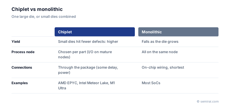
Why split a chip into chiplets
Yield is the first reason. Random defects are spread across the wafer, so the larger a die, the more likely it is to contain one and be scrapped. Several small dies yield better than one big die of the same total area, and each can be tested before assembly so that only known good dies are packaged. Very large designs also approach the reticle limit, the largest area a scanner can expose at once, which chiplets let them exceed.
The second reason is freedom of process. Logic cores benefit from the newest node, while I/O circuits, analog blocks and some SRAM shrink little and can stay on cheaper mature processes. The same chiplets can also be reused across a product range: a server processor and a desktop processor may share core dies and differ only in how many are fitted.
How chiplets are connected
The cost of splitting is the interface. Signals between dies travel through the package instead of on-chip wiring, which adds latency and energy, so chiplets use short, wide and dense links. Options range from fine-pitch wiring on organic substrates, to silicon interposers and embedded silicon bridges (TSMC CoWoS and InFO, Intel EMIB), to direct 3D stacking with micro-bumps or hybrid bonding (Intel Foveros, TSMC SoIC).
AMD's EPYC server processors combine several CPU core dies with a separate I/O die, Intel's Meteor Lake places compute, graphics and I/O tiles on a base die with Foveros, and Apple's M1 Ultra joins two M1 Max dies through a bridge. To let dies from different vendors work together, the industry formed the UCIe (Universal Chiplet Interconnect Express) consortium, which publishes an open die-to-die interface standard.
Japanese companies involved
- Toray Engineering makes flip-chip and die bonders, and Tokyo Electron supplies wafer bonding equipment used in 3D stacking.
- DISCO's grinding and dicing equipment is used to thin and singulate the dies, and IBIDEN makes the high-end package substrates on which multi-die processors are mounted.
- Toray Engineering · Flip-chip bonders, die bonders and visual inspection systems
- Tokyo Electron (TEL) · Coat/develop, etch and deposition equipment
- DISCO · Dicing, grinding and polishing equipment
- IBIDEN · IC package substrates (FC-BGA)
FAQ
What is the difference between a chiplet and an SoC?
An SoC integrates all functions on one die. A chiplet design spreads those functions over several dies in one package. The package as a whole can behave like an SoC, so the two are often described as monolithic versus disaggregated integration.
Do chiplet products already use UCIe?
Most chiplet products so far use each company's own die-to-die links, such as AMD's Infinity Fabric. UCIe, first published in 2022, aims to make chiplets from different suppliers interoperable, and products and IP supporting it are now appearing.
What is a known good die?
A die that has been tested and shown to work before it is assembled. In a package with many chiplets, one bad die can scrap the whole assembly, so wafer-level testing of each chiplet becomes more thorough than for single-die products.
Comparisons
Related pages
Sources
Last updated: November 2, 2026