Registration
Registration is the positional accuracy that shows how closely a written pattern is placed to its designed position on the ideal grid. The term most often refers to pattern placement on a photomask, also called image placement, and is controlled at the nanometre level.
Also called: pattern placement, image placement, mask registration
Diagram
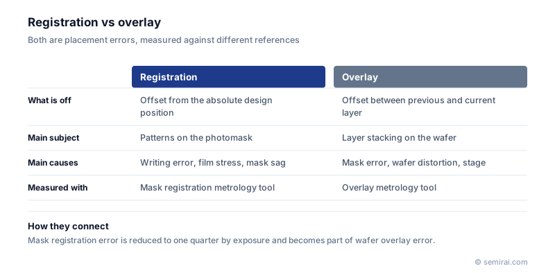
Registration vs overlay
Overlay is the misalignment between the pattern of the current layer and that of the previous layer on the wafer, a relative error between layers. Registration is an absolute error: how far a pattern on a single mask or wafer is displaced from where the design places it.
The two are linked. In a 4x reduction exposure tool, a registration error on the mask is shrunk to one quarter on the wafer and becomes one component of the wafer's overlay error. Older literature sometimes uses 'registration' to mean overlay, so context matters.
Causes and measurement of mask registration error
Mask registration errors come from positioning errors in the electron-beam mask writer, temperature drift and charging during writing, distortion caused by film stress on the mask, and sag that depends on how the mask is supported. Dedicated registration metrology tools measure the positions of many marks across the whole mask to correct and qualify it.
EUV masks are reflective, so the flatness of the mask and the condition of its back side also translate into placement errors. That makes registration control for EUV masks stricter than for conventional transmissive masks.
Japanese companies involved
- NuFlare Technology makes electron-beam mask writers, whose beam positioning accuracy is a primary factor in mask registration.
- NuFlare Technology · Electron-beam mask writers, mask inspection and epitaxial reactors
FAQ
Why does mask registration matter for chip yield?
Overlay budgets at advanced nodes are only a few nanometres, and the mask's placement error consumes part of that budget on every exposure. If the mask contributes too much, there is less margin left for the scanner and wafer distortion, and vias or contacts may miss the lines they should connect to.
Can registration errors be corrected?
Partly. Systematic errors measured on the mask can be fed back to the mask writer for the next mask, or compensated during exposure with the scanner's alignment and correction functions. Random, non-repeatable errors cannot be corrected and must be kept small at the writing stage.
Related pages
Sources
Last updated: November 13, 2026