Step-and-Repeat / Step-and-Scan
Step-and-repeat is an exposure method in which a mask pattern is printed onto one field (shot) of the wafer at once, the stage then steps to the next field and exposes again, and the cycle repeats over the whole wafer. Exposure tools that work this way are called steppers; step-and-scan tools, called scanners, sweep each field instead.
Also called: stepper, scanner, step and repeat exposure
Diagram
How steppers work
Steppers replaced whole-wafer exposure as the mainstream in the 1980s. The pattern on the mask, or reticle, is reduced by the projection lens, typically by a factor of four or five, so mask dimension errors shrink by the same factor and fine patterns are printed accurately.
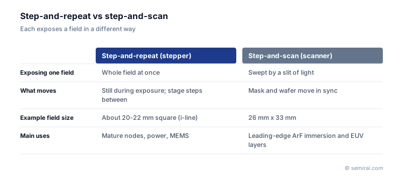
The field size that can be exposed in one shot is set by the lens. For i-line steppers it is a square of roughly 20-22 mm on a side.
Step-and-scan
Today's leading-edge tools use step-and-scan, a development of step-and-repeat. The mask and wafer move in opposite directions in synchrony beneath a narrow slit of light, exposing the field as they go; the stage then steps to the next field.
Only the best-corrected central strip of the lens is used, and the field can be made larger, 26 mm x 33 mm, so all ArF immersion and EUV exposure tools are scanners. i-line and KrF steppers are still used for mature nodes, power semiconductors and MEMS.
Japanese companies involved
- Nikon and Canon make i-line and KrF lithography tools; Nikon also makes ArF and ArF immersion scanners, while Canon is a major supplier of i-line steppers.
FAQ
What is the difference between a stepper and a scanner?
A stepper holds the mask and wafer still and exposes an entire field in one flash. A scanner illuminates only a slit and moves mask and wafer in opposite directions to sweep the field. Because the mask moves four times as fast as the wafer, scanners need very precise synchronised stages.
Are steppers still used?
Yes. i-line and KrF steppers remain in service where low cost, thick resists or large depth of focus matter more than the finest resolution, as in mature-node logic, power devices, MEMS and some image sensor layers. The finest layers of advanced chips are exposed on ArF immersion or EUV scanners.
Related pages
Sources
Last updated: November 1, 2026