Stochastic Effects (EUV)
EUV stochastic effects are random, unpredictable variations in pattern size, shape and defects on the wafer, caused by statistical fluctuation in the number of photons absorbed and by the randomness of chemical reactions in the resist. They matter most in EUV lithography, where each photon carries a lot of energy and so few photons are used per feature.
Also called: stochastics, EUV stochastic defects, photon shot noise
Diagram
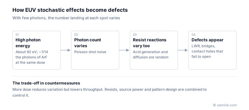
Why EUV is affected
An EUV photon at 13.5 nm carries about 92 eV, roughly fourteen times the energy of a 193 nm ArF photon. At the same dose, a feature therefore receives about one fourteenth as many photons. Photon arrival follows Poisson statistics, so the relative fluctuation grows as the count falls.
In the resist, the absorbed energy produces secondary electrons, which generate acids or trigger other reactions, and those acids diffuse. Each step adds randomness. Over millions of features, some receive too much or too little reaction and print wrongly.
How it shows up and what is done
The visible results are line edge and line width roughness, local critical-dimension variation, and stochastic defects such as bridges between lines, broken lines and contact holes that fail to open. Because a chip contains billions of features, even a very rare failure rate can kill yield, so stochastics often determine the dose and therefore the throughput of an EUV layer.
Countermeasures include raising the dose (at the cost of throughput), resists that absorb EUV more strongly or react more uniformly such as metal-oxide resists, better underlayers, design and optical proximity correction that avoid failure-prone shapes, and high-sensitivity inspection to measure failure rates. The effects grow more severe with High-NA EUV, which prints even smaller features.
Japanese companies involved
- JSR, Tokyo Ohka Kogyo (TOK) and Shin-Etsu Chemical develop EUV resists aimed at reducing roughness and stochastic defects; JSR owns Inpria, a developer of metal-oxide resists.
- Tokyo Ohka Kogyo (TOK) · Photoresists and high-purity process chemicals
- Shin-Etsu Chemical · Silicon wafers, photoresists and photomask blanks
- JSR · Photoresists and semiconductor materials
FAQ
Why can't the dose simply be raised?
Higher dose means longer exposure per field, which lowers the number of wafers an expensive EUV scanner can process per hour. Chipmakers balance the dose against throughput, which is why source power and resist sensitivity matter so much.
Do stochastic effects occur with DUV?
In principle yes, but at 193 nm a feature receives many more photons for the same dose, and features are larger, so the fluctuation is usually small compared with other error sources.
How are stochastic defects measured?
They are rare, so large areas must be inspected, typically with high-throughput electron-beam inspection or large CD-SEM samples, and failure rates are extrapolated statistically to the full chip.
Comparisons
Related pages
Sources
Lithography terms
- All lithography terms
- Swelling
- TMAH (Tetramethylammonium Hydroxide)
- EUV vs DUV lithography: what is the difference?
- High-NA EUV vs standard EUV: what is the difference?
- Single patterning vs multi-patterning: what is the difference?
- Chemically amplified resist vs metal oxide resist: what is the difference?
- Bottom Anti-Reflective Coating (BARC)
Last updated: November 2, 2026