Swirl Defect
Swirl defects are microscopic crystal defects that show up as a spiral or striped pattern when a slice of single-crystal silicon is selectively etched. They were found in dislocation-free float-zone (FZ) silicon in the 1960s and 1970s and later in Czochralski (CZ) crystal too. They line up with growth fluctuations, which is why they form a swirl.
Also called: swirl, A-defect, B-defect
Diagram
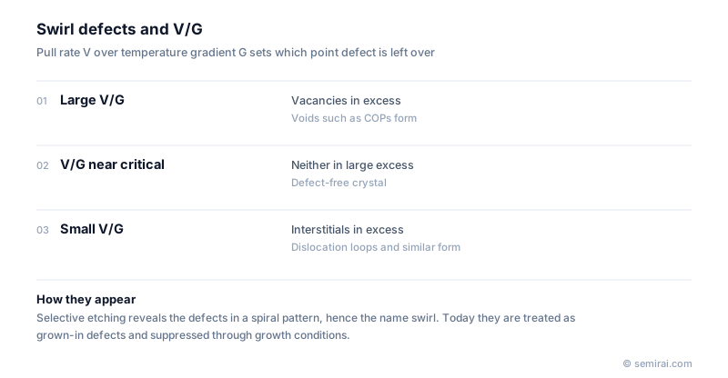
What swirl defects are
Swirl defects are clusters of point defects left over as the crystal cools: vacancies, where an atom is missing, or self-interstitials, extra silicon atoms between lattice sites. The larger defects formed by interstitials, which are dislocation loops, were called A-defects; smaller interstitial clusters were called B-defects.
Which type of point defect remains in excess is set by the ratio V/G, where V is the pull rate of the crystal and G is the temperature gradient near the solid-liquid interface. This was explained by Voronkov's theory. When V/G is large, vacancies dominate and form vacancy-type defects such as crystal-originated particles (COPs). When V/G is small, interstitials dominate and form interstitial-type defects. Near a critical value, neither species is left in large excess.
Why they matter and how they are controlled
Swirl defects cause junction leakage and oxide failures in devices built over them, so crystal makers worked to remove them by improving growth conditions. Today swirl defects and related defects formed during crystal growth are grouped as grown-in defects.
Wafer makers control them by precisely managing pull rate and temperature gradient to grow nearly defect-free crystal, or by covering or removing surface defects with high-temperature annealing or an epitaxial layer.
Japanese companies involved
- SUMCO and Shin-Etsu Chemical grow CZ silicon crystals and control grown-in defects through pull-rate and thermal design and through annealed and epitaxial wafer products.
- SUMCO · Silicon wafers
- Shin-Etsu Chemical · Silicon wafers, photoresists and photomask blanks
FAQ
Why do the defects form a spiral pattern?
The crystal rotates as it grows, and the growth rate and temperature fluctuate slightly and periodically. Defect density follows these fluctuations, so when the wafer is selectively etched, the defect-rich bands appear as stripes that form a swirl.
How are swirl defects different from COPs?
Both are grown-in defects. The A- and B-defects behind swirl patterns come from clustered silicon interstitials, while a COP is an octahedral void formed by clustered vacancies. Which one forms is decided by the V/G ratio during growth.
Related pages
Sources
Last updated: November 13, 2026