Wafer Flatness (TTV / SFQR / GBIR)
Wafer flatness is a set of metrics that describe how even the height of a wafer's surface is. Lithography focus depth is now only tens of nanometres, so small height variations can defocus the image and cause pattern defects. Flatness is therefore among the most important wafer specifications.
Also called: TTV, GBIR, SFQR, SBIR, site flatness
Diagram
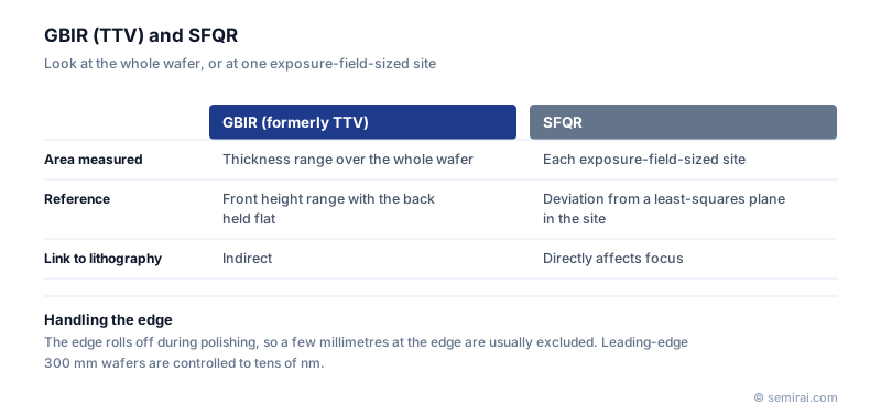
Global and site metrics
GBIR (global backside ideal range) is the difference between the highest and lowest points of the front surface across the whole wafer when the back surface is held ideally flat. It corresponds to the older term TTV (total thickness variation), the difference between maximum and minimum thickness. These global numbers matter for handling and chucking but are too coarse to judge lithography.
What matters for exposure is local flatness. SFQR (site front least-squares range) divides the wafer into rectangular sites the size of an exposure field, for example 26 × 8 mm, fits a least-squares plane to the front surface in each site and takes the range of deviation from that plane. The largest site value must meet the specification; for 300 mm wafers for leading-edge logic this is a few tens of nanometres. SBIR, a site metric referenced to the back surface, is also used.
Where flatness comes from
Flatness is built through slicing, lapping or double-side grinding, and double-side polishing (DSP). DSP processes the wafer without fixing it to a plate, which avoids copying the back surface shape and improves local flatness. Near the edge, polishing pressure changes and the surface rolls off. A few millimetres at the edge are therefore excluded from the specification (edge exclusion).
Flatness tools measure both faces at once with capacitive sensors or laser interferometry, with the wafer supported freely.
Japanese companies involved
- SUMCO and Shin-Etsu Chemical control flatness through double-side polishing and inspect every wafer against the customer's site flatness specification.
- Kobelco Research Institute makes wafer metrology equipment that measures flatness and shape.
- Kobelco Research Institute · Wafer metrology: flatness and carrier lifetime
- SUMCO · Silicon wafers
- Shin-Etsu Chemical · Silicon wafers, photoresists and photomask blanks
FAQ
How is flatness different from warp?
Warp and bow describe the curvature of the whole wafer when it is free. Chucking pulls that curvature flat. Flatness describes height variation that remains even when the wafer is chucked, which is why it directly affects lithography focus.
Does flatness matter after the wafer leaves the wafer maker?
Yes. Back grinding for packaging thins wafers and creates new thickness variation, and the tape or support used during grinding can transfer its own unevenness. TTV is therefore also controlled in back-end thinning.
Related pages
Sources
Last updated: November 13, 2026