Vertical Bridgman Method (VB)
The vertical Bridgman (VB) method grows a single crystal by moving a crucible of molten material slowly through a furnace with a temperature gradient, so the melt solidifies progressively upward from a seed crystal at the bottom. It is the vertical form of the method devised by the American physicist Percy Bridgman, and it is widely used for compound semiconductor substrates.
Also called: VB method, Bridgman-Stockbarger method
Diagram
VB, VGF and why they suit compound semiconductors
A closely related method, vertical gradient freeze (VGF), keeps both crucible and furnace still and instead changes the heater temperature profile over time so that the melt freezes from the bottom up. VB and VGF are used side by side.
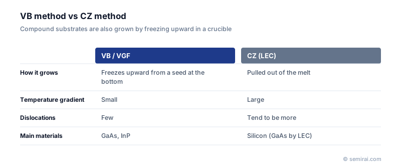
Both are used mainly to make gallium arsenide (GaAs) and indium phosphide (InP) single crystals. The Czochralski (CZ) method used for silicon pulls a crystal out of the melt, which creates large temperature differences inside the crystal. GaAs and InP are more fragile than silicon and form dislocations easily under thermal stress. VB and VGF solidify the crystal quietly inside the crucible with a small temperature gradient, so they give crystals with a lower dislocation density.
Arsenic and phosphorus evaporate easily, so the melt surface is covered with liquid boron oxide (B₂O₃), among other measures, to keep them in.
Uses and limitations
GaAs substrates made by VB or VGF are used for RF components in smartphones, LEDs, semiconductor lasers and VCSELs. InP substrates go into lasers and photodetectors for optical communication and into high-speed electronic devices.
Because the crystal solidifies in contact with the crucible wall, defects can start at the wall, and reaction or sticking between crucible and crystal must be prevented. Growth also takes a long time, and uniform temperature control becomes harder as crystal diameter increases.
Japanese companies involved
- Sumitomo Electric Industries makes GaAs and InP substrates and is known for growing GaAs by the VB method.
- JX Advanced Metals makes InP substrates for optical communication devices.
- Sumitomo Electric Industries (compound semiconductors) · SiC epitaxial wafers and GaAs and InP substrates
- JX Advanced Metals · Sputtering targets and high-purity metals
FAQ
What is the difference between VB and VGF?
In VB, the crucible and furnace move relative to each other so the melt passes into the cooler zone and solidifies. In VGF, nothing moves; the heater temperatures are lowered in a programmed way so the freezing front rises from the seed. VGF avoids mechanical motion, while VB can be simpler to control over long crystals.
What is LEC and how does it compare?
Liquid-encapsulated Czochralski (LEC) pulls GaAs from a melt covered with boron oxide, much like CZ silicon. It grows crystals quickly but with larger thermal gradients, so its crystals usually contain more dislocations than VB or VGF material.
Related pages
- Gallium Arsenide (GaAs)
- Indium Phosphide (InP)
- Czochralski Process (CZ Method)
- Compound Semiconductor
- Dislocation
- Seed Crystal
- PVT (Physical Vapour Transport) Method
- Temperature Gradient Method
- Crystal growth furnaces
- Compound semiconductor substrate equipment (SiC/GaN)
- Daiichi Kiden Round-Chamber Crystal Puller (CZ Method)
- Daiichi Kiden S278 / S380
- Daiichi Kiden Solution Growth System
- Ferrotec FT-CZ1200SE/1400SE
Sources
Last updated: November 13, 2026