Crystal Defect (Lattice Defect)
A crystal defect, or lattice defect, is any place where the regular periodic arrangement of atoms in a crystal is broken. Defects are classified by dimension into point, line, planar and volume defects. In semiconductors they create energy levels in the band gap that cause leakage and shorten carrier lifetime, yet some are engineered deliberately, for example to trap metal contamination.
Also called: lattice defect, point defect, planar defect, volume defect
Diagram
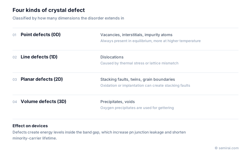
Four kinds by dimension
Point defects involve single atomic sites: vacancies (missing atoms), self-interstitials (extra atoms between sites) and impurity atoms on or between lattice sites. Dopants are intended point defects. Line defects are dislocations. Planar defects include stacking faults, where the layer sequence is interrupted, twin boundaries and the grain boundaries of polycrystalline material. Volume defects are three-dimensional, such as oxygen precipitates in Czochralski silicon, voids and inclusions.
Where defects come from
Point defects exist even in a perfect crystal in thermal equilibrium, and their number rises steeply with temperature. During crystal growth, the ratio of pull speed to temperature gradient decides whether vacancies or interstitials dominate as the ingot cools; excess vacancies cluster into tiny voids known as crystal-originated particles (COPs). Dislocations and stacking faults do not exist in equilibrium and are created by thermal stress, lattice mismatch or process steps.
Processing adds more. Ion implantation knocks atoms out of place, and annealing can leave dislocation loops at the end of the implanted range. Thermal oxidation injects interstitials that can form oxidation-induced stacking faults. Small defects often grow into larger ones as excess point defects gather.
Effects on devices and how defects are used
Levels in the band gap act as traps and recombination centres. They raise pn junction leakage, shorten DRAM retention, create dark current and white spots in image sensors and reduce minority-carrier lifetime in solar cells. Metal contamination that decorates defects makes the effect worse. Epitaxial and hydrogen- or argon-annealed wafers keep the near-surface device layer free of grown-in defects.
Defects are also put to work. In intrinsic gettering, oxygen precipitates are grown deep in the wafer to trap iron, copper and nickel, while the surface is left as a defect-free denuded zone. Power diodes are given recombination centres by platinum diffusion or electron irradiation to switch off faster.
Japanese companies involved
- Shin-Etsu Chemical and SUMCO make epitaxial and annealed silicon wafers designed to keep the device layer free of grown-in defects.
- Rigaku makes X-ray diffraction and topography systems used to evaluate defects in wafers and epitaxial layers.
- Shin-Etsu Chemical · Silicon wafers, photoresists and photomask blanks
- SUMCO · Silicon wafers
- Rigaku · X-ray metrology and thermal analysis
FAQ
Are 'lattice defect' and 'crystal defect' the same?
They are used almost interchangeably. Some texts reserve 'lattice defect' for disorder of the atomic arrangement itself, such as point defects and dislocations, and do not include precipitates of a second phase.
Can crystal defects be eliminated completely?
No. Vacancies and interstitials exist at any temperature above absolute zero. Defects that are not in equilibrium, such as dislocations and stacking faults, can be reduced to levels devices tolerate, and silicon ingots are produced in volume without dislocations.
How are defects in wafers detected?
Laser light-scattering inspection finds surface particles and pits, selective etching reveals stacking faults and dislocations as countable features, and X-ray topography maps strain and dislocations nondestructively. Lifetime measurements detect electrically active defects and metal contamination.
Related pages
Sources
Last updated: November 13, 2026