Czochralski Process (CZ Method)
The Czochralski process (CZ method) is the standard technique for growing the single-crystal silicon ingots from which semiconductor wafers are cut. High-purity silicon is melted in a quartz crucible, a seed crystal is dipped into the melt, and it is slowly pulled upward while rotating, so the growing crystal copies the seed's orientation.
Also called: CZ method, CZ growth, crystal pulling
Diagram
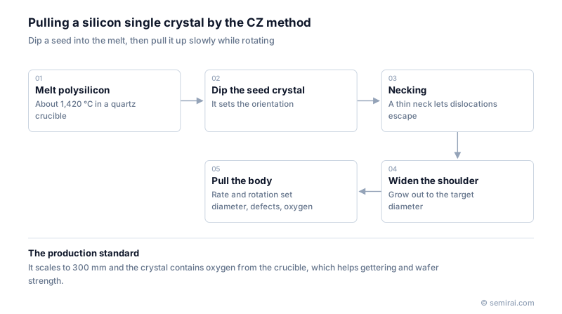
How the crystal is pulled
Polycrystalline silicon is loaded into a quartz crucible inside a graphite-heated furnace filled with argon and melted at just above the melting point of silicon, around 1,420 °C. A small seed crystal cut to the required orientation is lowered until it touches the melt surface. The crystal is first pulled into a thin neck a few millimetres wide, which lets the dislocations created by thermal shock grow out to the surface. The diameter is then widened through a shoulder to the target size and the cylindrical body is pulled at constant diameter.
The pull rate, the rotation of the crystal and the crucible, and the temperature gradient near the growth interface are controlled together. These settings decide the diameter, the type and density of crystal defects, the oxygen content and, through the dopant added to the melt, the resistivity.
Oxygen and other characteristics
Because the melt is held in quartz (SiO₂), some oxygen dissolves from the crucible wall and enters the crystal. This is the defining feature of CZ silicon. The oxygen can be turned into precipitates that capture metal contamination (gettering) and it strengthens the wafer against slip, but for some devices it has to be kept within tight limits.
Applying a magnetic field to the melt (magnetic CZ, or MCZ) suppresses convection and gives better control of oxygen and its distribution. Almost all 300 mm wafers are cut from CZ ingots, because the method scales to large diameters and long crystals.
From ingot to wafer
After growth, the ingot is ground to an exact diameter, notched to mark its orientation, sliced with a wire saw, lapped or ground, etched, polished to a mirror finish and cleaned. The crucible-free float zone method is used instead when very low oxygen and high resistivity are needed.
Japanese companies involved
- Shin-Etsu Chemical (through Shin-Etsu Handotai) and SUMCO grow CZ silicon crystals and supply polished, epitaxial and other silicon wafers to chipmakers worldwide.
- Shin-Etsu Quartz Products makes high-purity quartz glass products, including crucibles of the kind used to hold the silicon melt.
- Shin-Etsu Quartz Products · High-purity quartz glass parts and crucibles
- Shin-Etsu Chemical · Silicon wafers, photoresists and photomask blanks
- SUMCO · Silicon wafers
FAQ
Why is CZ silicon used for almost all large wafers?
The CZ process can grow crystals of 300 mm diameter and about two metres long at a practical rate. The float zone method has no crucible to support the melt, so it becomes very difficult at large diameters.
Is the oxygen in CZ silicon a defect?
It is an impurity, but a useful one in controlled amounts. Oxygen precipitates inside the wafer trap metals away from the surface and oxygen pins dislocations, making the wafer stronger during high-temperature steps. Too much oxygen, however, can form thermal donors that shift resistivity.
Comparisons
Related pages
Sources
Last updated: November 2, 2026