Wafer Bow and Warp
Bow and warp describe how much a wafer is curved when it rests freely, without being clamped. Bow is the signed distance of the centre of the median surface from a reference plane, so it shows whether the wafer is convex or concave. Warp is the difference between the highest and lowest points of that surface, including any waviness.
Also called: bow, warp, wafer warpage
Diagram
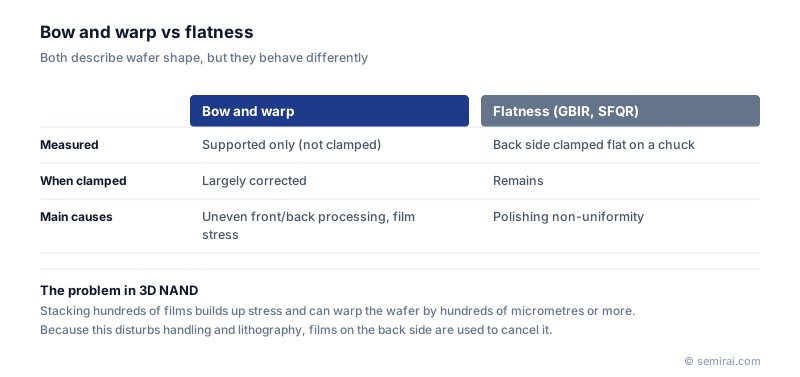
Bow, warp and flatness
Both values are measured on the median surface, halfway between front and back, so that thickness variation does not count as curvature. A wafer shaped like a shallow dish has bow and warp of similar size. A wafer shaped like a saddle or a potato chip can have almost no bow but a large warp, which is why both are specified. SEMI MF1390 describes how they are measured by automated non-contact scanning.
Flatness metrics such as GBIR and SFQR are different. They are measured with the back of the wafer held flat on a chuck and describe thickness variation of the front surface, which remains after clamping. Bow and warp, by contrast, are largely removed when the wafer is clamped, until they become too large for the chuck to correct.
Where warp comes from
In wafer manufacturing, warp comes from uneven processing of the two faces: deflection of the saw wire during slicing, different amounts removed from each side during lapping and polishing, and temperature gradients during heat treatment. Any imbalance of residual stress between front and back bends the wafer once it is free. Double-side polishing is used partly because treating both faces equally avoids this imbalance.
In device fabrication, thin-film stress takes over. A film under tension or compression, or one that contracts differently from silicon on cooling, bends the wafer, and the Stoney equation relates the change in curvature to the film stress. Thick stacks of many layers, as in 3D NAND, thick metal films and back-side electrodes on thinned power wafers can produce bow or warp of hundreds of micrometres or more.
Why it matters
A strongly warped wafer may not seal on a vacuum or electrostatic chuck, may be picked up wrongly by a transfer robot, or may break after thinning. If a lithography chuck flattens it by force, the surface stretches in-plane and causes overlay errors. Fabs counter this with stress-balancing films on the back side, tuned deposition conditions and careful stacking order.
Japanese companies involved
- Shin-Etsu Chemical and SUMCO make silicon wafers and control bow and warp through their slicing, lapping and double-side polishing processes.
- SUMCO · Silicon wafers
- Shin-Etsu Chemical · Silicon wafers, photoresists and photomask blanks
FAQ
How are bow and warp measured?
The wafer is supported at three points or by a small area near its centre, and capacitive sensors or optical interferometers scan both surfaces to build a thickness-independent map of the median surface. Gravity sag is corrected so that the result reflects the wafer's own shape.
Can film stress be measured from wafer bow?
Yes. Measuring curvature before and after deposition and applying the Stoney equation, with the substrate's thickness and elastic properties, gives the average stress of the film. This is a routine monitor in deposition processes.
Why are thinned wafers more sensitive to warp?
By the Stoney equation, the curvature caused by a given film grows with the inverse square of the wafer thickness, so halving the thickness roughly quadruples the bending. Thinned wafers are therefore often bonded to a carrier or kept on a frame while they are handled.
Related pages
- Wafer Flatness (TTV / SFQR / GBIR)
- Wafer Thinning
- Wafer Bonding
- 3D NAND Flash
- Plastic Deformation
- Coefficient of Thermal Expansion (CTE)
- Package Warpage
- End Effector (Wafer Robot Hand)
- Wafer polishing and edge grinding equipment
- DISCO DFP8141
- Fujikoshi Machinery MCP-200
- Fujikoshi Machinery SPM-23
- Komatsu NTC GCG300
Sources
Wafers and substrates terms
Last updated: November 13, 2026